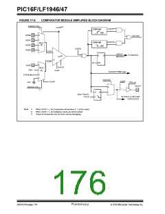
PIC16F/LF1946/47
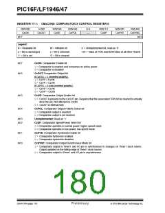
REGISTER 17-1: CMxCON0: COMPARATOR X CONTROL REGISTER 0
R/W-0/0
CxON
R-0/0
R/W-0/0
CxOE
R/W-0/0
CxPOL
U-0
—
R/W-1/1
CxSP
R/W-0/0
CxHYS
R/W-0/0
CxSYNC
CxOUT
bit 7
bit 0
Legend:
R = Readable bit
W = Writable bit
U = Unimplemented bit, read as ‘0’
-n/n = Value at POR and BOR/Value at all other Resets
u = Bit is unchanged
‘1’ = Bit is set
x = Bit is unknown
‘0’ = Bit is cleared
bit 7
bit 6
CxON: Comparator Enable bit
1= Comparator is enabled and consumes no active power
0= Comparator is disabled
CxOUT: Comparator Output bit
If CxPOL = 1 (inverted polarity):
1= CxVP < CxVN
0= CxVP > CxVN
If CxPOL = 0 (non-inverted polarity):
1= CxVP > CxVN
0= CxVP < CxVN
bit 5
bit 4
CxOE: Comparator Output Enable bit
1= CxOUT is present on the CxOUT pin. Requires that the associated TRIS bit be cleared to actually
drive the pin. Not affected by CxON.
0= CxOUT is internal only
CxPOL: Comparator Output Polarity Select bit
1= Comparator output is inverted
0= Comparator output is not inverted
bit 3
bit 2
Unimplemented: Read as ‘0’
CxSP: Comparator Speed/Power Select bit
1= Comparator operates in normal power, higher speed mode
0= Comparator operates in low-power, low-speed mode
bit 1
bit 0
CxHYS: Comparator Hysteresis Enable bit
1= Comparator hysteresis enabled
0= Comparator hysteresis disabled
CxSYNC: Comparator Output Synchronous Mode bit
1= Comparator output to Timer1 and I/O pin is synchronous to changes on Timer1 clock source.
Output updated on the falling edge of Timer1 clock source.
0= Comparator output to Timer1 and I/O pin is asynchronous
DS41414A-page 178
Preliminary
2010 Microchip Technology Inc.

 MICROCHIP [ MICROCHIP ]