PIC16F/LF1946/47
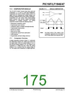
17.3 Comparator Hysteresis
17.5 Comparator Interrupt
A selectable amount of separation voltage can be
added to the input pins of each comparator to provide a
hysteresis function to the overall operation. Hysteresis
is enabled by setting the CxHYS bit of the CMxCON0
register.
An interrupt can be generated upon a change in the
output value of the comparator for each comparator, a
rising edge detector and a Falling edge detector are
present.
When either edge detector is triggered and its associ-
ated enable bit is set (CxINTP and/or CxINTN bits of
the CMxCON1 register), the Corresponding Interrupt
Flag bit (CxIF bit of the PIR2 register) will be set.
These hysteresis levels change as a function of the
comparator’s Speed/Power mode selection.
Table 17-2 shows the hysteresis levels.
To enable the interrupt, you must set the following bits:
• CxON, CxPOL and CxSP bits of the CMxCON0
register
TABLE 17-2: HYSTERESIS LEVELS
CxSP
CxHYS Enabled CxHYS Disabled
• CxIE bit of the PIE2 register
0
1
± 3mV
<< ± 1mV
± 3mV
• CxINTP bit of the CMxCON1 register (for a rising
edge detection)
± 20mV
• CxINTN bit of the CMxCON1 register (for a falling
edge detection)
These levels are approximate.
See Section 29.0 “Electrical Specifications” for
more information.
• PEIE and GIE bits of the INTCON register
The associated interrupt flag bit, CxIF bit of the PIR2
register, must be cleared in software. If another edge is
detected while this flag is being cleared, the flag will still
be set at the end of the sequence.
17.4 Timer1 Gate Operation
The output resulting from a comparator operation can
be used as a source for gate control of Timer1. See
Section 20.6 “Timer1 Gate” for more information.
This feature is useful for timing the duration or interval
of an analog event.
Note:
Although a comparator is disabled, an
interrupt can be generated by changing
the output polarity with the CxPOL bit of
the CMxCON0 register, or by switching the
comparator on or off with the CxON bit of
the CMxCON0 register.
It is recommended that the comparator output be
synchronized to Timer1. This ensures that Timer1 does
not increment while a change in the comparator is
occurring.
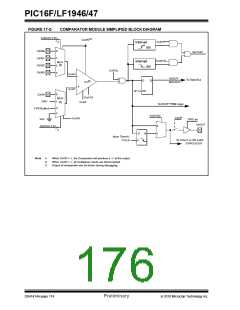
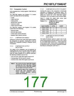
17.6 Comparator Positive Input
Selection
17.4.1
COMPARATOR OUTPUT
SYNCHRONIZATION
Configuring the CxPCH<1:0> bits of the CMxCON1
register directs an internal voltage reference or an
analog pin to the non-inverting input of the comparator:
The output from a comparator can be synchronized
with Timer1 by setting the CxSYNC bit of the
CMxCON0 register.
• CxIN+ analog pin
• DAC
Once enabled, the comparator output is latched on the
falling edge of the Timer1 source clock. If a prescaler is
used with Timer1, the comparator output is latched after
the prescaling function. To prevent a race condition, the
comparator output is latched on the falling edge of the
Timer1 clock source and Timer1 increments on the
rising edge of its clock source. See the Comparator
Block Diagram (Figure 17-2) and the Timer1 Block
Diagram (Figure 20-1) for more information.
• FVR (Fixed Voltage Reference)
• VSS (Ground)
See Section 14.0 “Fixed Voltage Reference (FVR)”
for more information on the Fixed Voltage Reference
module.
See Section 16.0 “Digital-to-Analog Converter
(DAC) Module” for more information on the DAC input
signal.
Any time the comparator is disabled (CxON = 0), all
comparator inputs are disabled.
DS41414A-page 176
Preliminary
2010 Microchip Technology Inc.

 MICROCHIP [ MICROCHIP ]