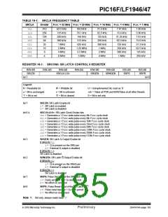
PIC16F/LF1946/47
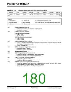
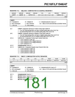
REGISTER 17-2: CMxCON1: COMPARATOR CX CONTROL REGISTER 1
R/W-0/0
CxINTP
R/W-0/0
CxINTN
R/W-0/0
R/W-0/0
U-0
—
U-0
—
R/W-0/0
R/W-0/0
CxPCH<1:0>
CxNCH<1:0>
bit 7
bit 0
Legend:
R = Readable bit
W = Writable bit
U = Unimplemented bit, read as ‘0’
-n/n = Value at POR and BOR/Value at all other Resets
u = Bit is unchanged
‘1’ = Bit is set
x = Bit is unknown
‘0’ = Bit is cleared
bit 7
CxINTP: Comparator Interrupt on Positive Going Edge Enable bit
1= The CxIF interrupt flag will be set upon a positive going edge of the CxOUT bit
0= No interrupt flag will be set on a positive going edge of the CxOUT bit
bit 6
CxINTN: Comparator Interrupt on Negative Going Edge Enable bit
1= The CxIF interrupt flag will be set upon a negative going edge of the CxOUT bit
0= No interrupt flag will be set on a negative going edge of the CxOUT bit
bit 5-4
CxPCH<1:0>: Comparator Positive Input Channel Select bits
00= CxVP connects to CxIN+ pin
01= CxVP connects to DAC Voltage Reference
10= CxVP connects to FVR Voltage Reference
11= CxVP connects to VSS
bit 3-2
bit 1-0
Unimplemented: Read as ‘0’
CxNCH<1:0>: Comparator Negative Input Channel Select bits
00= CxVN connects to CxIN0- pin
01= CxVN connects to CxIN1- pin
10= CxVN connects to CxIN2- pin
11= CxVN connects to CxIN3- pin
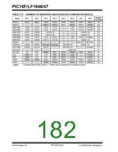
REGISTER 17-3: CMOUT: COMPARATOR OUTPUT REGISTER
U-0
—
U-0
—
U-0
—
U-0
—
U-0
—
R-0/0
R-0/0
R-0/0
MC3OUT
MC2OUT
MC1OUT
bit 7
bit 0
Legend:
R = Readable bit
W = Writable bit
x = Bit is unknown
‘0’ = Bit is cleared
U = Unimplemented bit, read as ‘0’
-n/n = Value at POR and BOR/Value at all other Resets
u = Bit is unchanged
‘1’ = Bit is set
bit 7-3
bit 2
Unimplemented: Read as ‘0’
MC3OUT: Mirror Copy of C3OUT bit
MC2OUT: Mirror Copy of C2OUT bit
MC1OUT: Mirror Copy of C1OUT bit
bit 1
bit 0
2010 Microchip Technology Inc.
Preliminary
DS41414A-page 179

 MICROCHIP [ MICROCHIP ]