PIC16F/LF1946/47
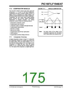
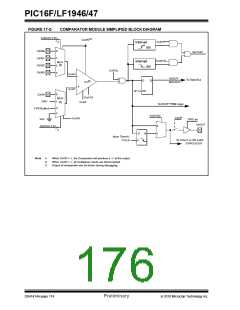
FIGURE 17-2:
COMPARATOR MODULE SIMPLIFIED BLOCK DIAGRAM
CxNCH<1:0>
CxON(1)
2
CxINTP
Interrupt
det
0
CXIN0-
CXIN1-
CXIN2-
CXIN3-
Set CxIF
1
CxINTN
Interrupt
det
MUX
(2)
2
3
CXPOL
CxVN
CxVP
-
CXOUT
To Data Bus
D
Q
Cx(3)
MCXOUT
+
Q1
EN
0
CXIN+
CxHYS
MUX
DAC
1
(2)
CxSP
To ECCP PWM Logic
2
3
FVR Buffer2
CXSYNC
CXOE
CxON
VSS
TRIS bit
CXOUT
CXPCH<1:0>
0
1
2
D
Q
(from Timer1)
T1CLK
To Timer1 or SR Latch
SYNCCXOUT
Note 1:
When CxON = 0, the Comparator will produce a ‘0’ at the output.
When CxON = 0, all multiplexer inputs are disconnected.
Output of comparator can be frozen during debugging.
2:
3:
DS41414A-page 174
Preliminary
2010 Microchip Technology Inc.

 MICROCHIP [ MICROCHIP ]