PIC16F/LF1946/47
17.2.3
COMPARATOR OUTPUT POLARITY
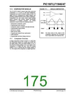
17.2 Comparator Control
Inverting the output of the comparator is functionally
equivalent to swapping the comparator inputs. The
polarity of the comparator output can be inverted by
setting the CxPOL bit of the CMxCON0 register.
Clearing the CxPOL bit results in a non-inverted output.
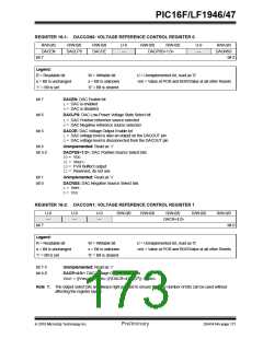
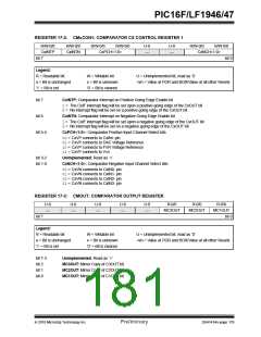
Each comparator has 2 control registers: CMxCON0 and
CMxCON1.
The CMxCON0 registers (see Register 17-1) contain
Control and Status bits for the following:
• Enable
Table 17-1 shows the output state versus input
conditions, including polarity control.
• Output selection
• Output polarity
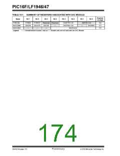
TABLE 17-1: COMPARATOR OUTPUT
STATE VS. INPUT
• Speed/Power selection
• Hysteresis enable
• Output synchronization
CONDITIONS
Input Condition
CxPOL
CxOUT
The CMxCON1 registers (see Register 17-2) contain
Control bits for the following:
CxVN > CxVP
CxVN < CxVP
CxVN > CxVP
CxVN < CxVP
0
0
1
1
0
1
0
1
• Interrupt enable
• Interrupt edge polarity
• Positive input channel selection
• Negative input channel selection
17.2.4
COMPARATOR SPEED/POWER
SELECTION
17.2.1
COMPARATOR ENABLE
The trade-off between speed or power can be opti-
mized during program execution with the CxSP control
bit. The default state for this bit is ‘1’ which selects the
normal speed mode. Device power consumption can
be optimized at the cost of slower comparator propaga-
tion delay by clearing the CxSP bit to ‘0’.
Setting the CxON bit of the CMxCON0 register enables
the comparator for operation. Clearing the CxON bit
disables the comparator resulting in minimum current
consumption.
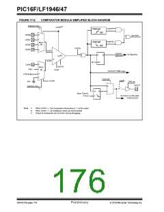
17.2.2
COMPARATOR OUTPUT
SELECTION
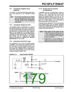
The output of the comparator can be monitored by
reading either the CxOUT bit of the CMxCON0 register
or the MCxOUT bit of the CMOUT register. In order to
make the output available for an external connection,
the following conditions must be true:
• CxOE bit of the CMxCON0 register must be set
• Corresponding TRIS bit must be cleared
• CxON bit of the CMxCON0 register must be set
Note 1: The CxOE bit of the CMxCON0 register
overrides the PORT data latch. Setting
the CxON bit of the CMxCON0 register
has no impact on the port override.
2: The internal output of the comparator is
latched with each instruction cycle.
Unless otherwise specified, external
outputs are not latched.
2010 Microchip Technology Inc.
Preliminary
DS41414A-page 175

 MICROCHIP [ MICROCHIP ]