PIC16F/LF1946/47
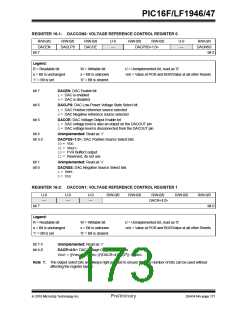
REGISTER 16-1: DACCON0: VOLTAGE REFERENCE CONTROL REGISTER 0
R/W-0/0
DACEN
R/W-0/0
DACLPS
R/W-0/0
DACOE
U-0
—
R/W-0/0
R/W-0/0
U-0
—
R/W-0/0
DACPSS<1:0>
DACNSS
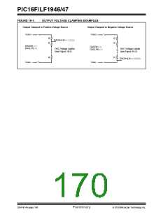
bit 7
bit 0
Legend:
R = Readable bit
W = Writable bit
x = Bit is unknown
‘0’ = Bit is cleared
U = Unimplemented bit, read as ‘0’
-n/n = Value at POR and BOR/Value at all other Resets
u = Bit is unchanged
‘1’ = Bit is set
bit 7
bit 6
DACEN: DAC Enable bit
1= DAC is enabled
0= DAC is disabled
DACLPS: DAC Low-Power Voltage State Select bit
1= DAC Positive reference source selected
0= DAC Negative reference source selected
bit 5
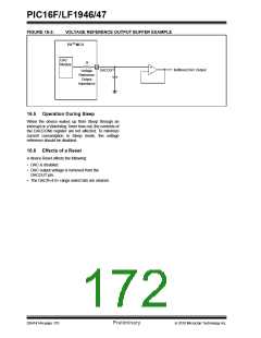
DACOE: DAC Voltage Output Enable bit
1= DAC voltage level is also an output on the DACOUT pin
0= DAC voltage level is disconnected from the DACOUT pin
bit 4
Unimplemented: Read as ‘0’
bit 3-2
DACPSS<1:0>: DAC Positive Source Select bits
00= VDD
01= VREF+
10= FVR Buffer2 output
11= Reserved, do not use
bit 1
bit 0
Unimplemented: Read as ‘0’
DACNSS: DAC Negative Source Select bits
1= VREF-
0= VSS
REGISTER 16-2: DACCON1: VOLTAGE REFERENCE CONTROL REGISTER 1
U-0
—
U-0
—
U-0
—
R/W-0/0
R/W-0/0
R/W-0/0
R/W-0/0
R/W-0/0
bit 0
DACR<4:0>
bit 7
Legend:
R = Readable bit
u = Bit is unchanged
‘1’ = Bit is set
W = Writable bit
U = Unimplemented bit, read as ‘0’
-n/n = Value at POR and BOR/Value at all other Resets
x = Bit is unknown
‘0’ = Bit is cleared
bit 7-5
bit 4-0
Unimplemented: Read as ‘0’
DACR<4:0>: DAC Voltage Output Select bits
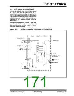
VOUT = ((VSRC+) - (VSRC-))*(DACR<4:0>/(25)) + VSRC-
Note 1: The output select bits are always right justified to ensure that any number of bits can be used without
affecting the register layout.
2010 Microchip Technology Inc.
Preliminary
DS41414A-page 171

 MICROCHIP [ MICROCHIP ]