PIC12F635/PIC16F636/639
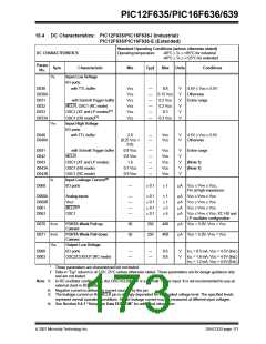
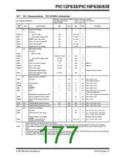
15.5 DC Characteristics: PIC16F639-I (Industrial)
Standard Operating Conditions (unless otherwise stated)
Operating temperature -40°C ≤ TA ≤ +85°C for industrial
DC CHARACTERISTICS
Param
Sym
Characteristic
Min Typ† Max Units
Conditions
No.
D001
VDD
Supply Voltage
2.0
2.0
—
—
3.6
3.6
V
V
FOSC ≤ 10 MHz
D001A VDDT
Supply Voltage (AFE)
Analog Front-End VDD voltage. Treated as
VDD in this document.
D002
D003
VDR
RAM Data Retention
Voltage(1)
1.5*
—
—
—
—
V
V
Device in Sleep mode
VPOR
VDD Start Voltage to
ensure internal Power-on
Reset signal
VSS
See Section 12.3 “Power-on Reset” for
details.
D003A VPORT VDD Start Voltage (AFE)
to ensure internal Power-
—
—
—
1.8
—
V
Analog Front-End POR voltage.
on Reset signal
D004
SVDD
VDD Rise Rate to ensure 0.05*
internal Power-on Reset
signal
V/ms See Section 12.3 “Power-on Reset” for
details.
D005
D006
VBOD
RM
Brown-out Reset
2.0
—
2.1
50
2.2
V
Turn-on Resistance or
100 Ohm VDD = 3.0V
Modulation Transistor
D007
D008
RPU
IAIL
Digital Input Pull-Up
Resistor
CS, SCLK
50
200 350 kOhm VDD = 3.6V
Analog Input Leakage
Current
LCX, LCY, LCZ
LCCOM
—
—
—
—
±1
±1
μA
μA
VDD = 3.6V, VSS ≤ VIN ≤ VDD, tested at
Sleep mode
*
These parameters are characterized but not tested.
†
Data in “Typ” column is at 3.0V, 25°C unless otherwise stated. These parameters are for design guidance
only and are not tested.
Note 1: This is the limit to which VDD can be lowered in Sleep mode without losing RAM data.
© 2007 Microchip Technology Inc.
DS41232D-page 173

 MICROCHIP [ MICROCHIP ]