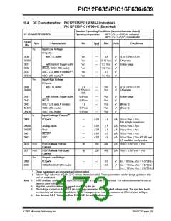
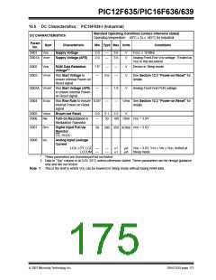
PIC12F635/PIC16F636/639
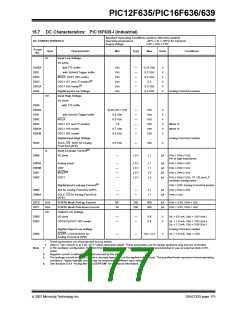
15.7 DC Characteristics: PIC16F639-I (Industrial)
Standard Operating Conditions (unless otherwise stated)
DC CHARACTERISTICS
Operating temperature
Supply Voltage
-40°C ≤ TA ≤ +85°C for industrial
2.0V ≤ VDD ≤ 3.6V
Param
Sym
No.
Characteristic
Min
Typ†
Max
Units
Conditions
VIL
Input Low Voltage
I/O ports:
with TTL buffer
D030A
D031
D032
D033
D033A
D034
VSS
VSS
VSS
VSS
VSS
VSS
—
—
—
—
—
—
0.15 VDD
0.2 VDD
0.2 VDD
0.3
V
V
V
V
V
V
with Schmitt Trigger buffer
MCLR, OSC1 (RC mode)
OSC1 (XT and LP modes)(1)
OSC1 (HS mode)(1)
0.3 VDD
0.3 VDD
Digital Input Low Voltage
Input High Voltage
Analog Front-End section
VIH
I/O ports:
D040
with TTL buffer
D040A
D041
(0.25 VDD + 0.8)
0.8 VDD
0.8 VDD
1.6
—
—
—
—
—
—
VDD
VDD
VDD
VDD
VDD
VDD
V
V
V
V
V
V
with Schmitt Trigger buffer
MCLR
D042
D043
OSC1 (XT and LP modes)
OSC1 (HS mode)
(Note 1)
(Note 1)
D043A
D043B
0.7 VDD
0.9 VDD
OSC1 (RC mode)
Digital Input High Voltage
Analog Front-End section
D044
D060
SCLK, CS, SDIO for Analog
Front-End (AFE)
Input Leakage Current(2)
0.8 VDD
—
VDD
V
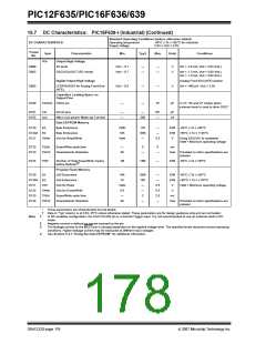
IIL
I/O ports
—
0.1
1
μA
VSS ≤ VPIN ≤ VDD,
Pin at high-impedance
D060A
D060B
D061
Analog inputs
VREF
MCLR(3)
—
—
—
—
0.1
0.1
0.1
0.1
1
1
5
5
μA
μA
μA
μA
VSS ≤ VPIN ≤ VDD
VSS ≤ VPIN ≤ VDD
VSS ≤ VPIN ≤ VDD
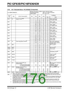
D063
OSC1
VSS ≤ VPIN ≤ VDD, XT, HS and LP
oscillator configuration
Digital Input Leakage Current(2)
VDD = 3.6V, Analog Front-End section
VSS ≤ VPIN ≤ VDD
D064
SDI for Analog Front-End (AFE)
—
—
—
—
1
1
μA
μA
D064A
SCLK, CS for Analog Front-End
(AFE)
VPIN ≤ VDD
D070
D071
IPUR
IPDR
VOL
PORTA Weak Pull-up Current
PORTA Weak Pull-down Current
Output Low Voltage
50*
50
250
250
400
400
μA
μA
VDD = 3.6V, VPIN = VSS
VDD = 3.6V, VPIN = VDD
D080
D083
I/O ports
—
—
—
—
0.6
0.6
V
V
IOL = 8.5 mA, VDD = 3.6V (Ind.)
OSC2/CLKOUT (RC mode)
IOL = 1.6 mA, VDD = 3.6V (Ind.)
IOL = 1.2 mA, VDD = 3.6V (Ext.)
Digital Output Low Voltage
Analog Front-End section
IOL = 1.0 mA, VDD = 2.0V
D084
ALERT, LFDATA/SDIO for
Analog Front-End (AFE)
—
—
VSS + 0.4
V
*
These parameters are characterized but not tested.
†
Data in “Typ” column is at 3.0V, 25°C unless otherwise stated. These parameters are for design guidance only and are not tested.
In RC oscillator configuration, the OSC1/CLKIN pin is a Schmitt Trigger input. It is not recommended to use an external clock in RC
mode.
Note 1:
2:
3:
Negative current is defined as current sourced by the pin.
The leakage current on the MCLR pin is strongly dependent on the applied voltage level. The specified levels represent normal operating
conditions. Higher leakage current may be measured at different input voltages.
See Section 9.4.1 “Using the Data EEPROM” for additional information
4:
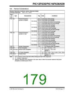
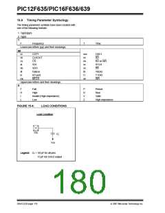
© 2007 Microchip Technology Inc.
DS41232D-page 175

 MICROCHIP [ MICROCHIP ]