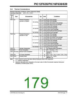
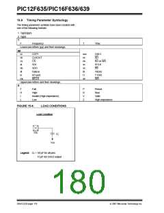
PIC12F635/PIC16F636/639
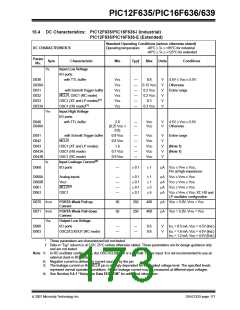
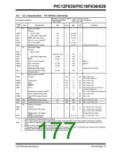
15.6 DC Characteristics: PIC16F639-I (Industrial)
Standard Operating Conditions (unless otherwise stated)
DC CHARACTERISTICS
Operating temperature
Supply Voltage
-40°C ≤ TA ≤ +85°C for industrial
2.0V ≤ VDD ≤ 3.6V
Conditions
Param
Sym
No.
Device Characteristics
Supply Current(1,2,3)
Min
Typ†
Max
Units
VDD
Note
D010
D011
D012
D013
D014
D015
D016
D017
D020
IDD
—
—
—
—
—
—
—
—
—
—
—
—
—
—
—
—
—
—
11
18
16
28
μA
μA
μA
μA
μA
μA
μA
μA
μA
μA
μA
μA
μA
μA
μA
μA
μA
μA
2.0
3.0
2.0
3.0
2.0
3.0
2.0
3.0
2.0
3.0
2.0
3.0
2.0
3.0
2.0
3.0
2.0
3.0
FOSC = 32.768 kHz
LP Oscillator mode
140
220
260
420
130
215
220
375
8
240
380
360
650
220
360
340
550
20
FOSC = 1 MHz
XT Oscillator mode
FOSC = 4 MHz
XT Oscillator mode
FOSC = 1 MHz
EC Oscillator mode
FOSC = 4 MHz
EC Oscillator mode
FOSC = 31 kHz
LFINTOSC mode
16
40
340
500
230
400
0.15
0.20
450
700
400
680
1.2
1.5
FOSC = 4 MHz
HFINTOSC mode
FOSC = 4 MHz
EXTRC mode
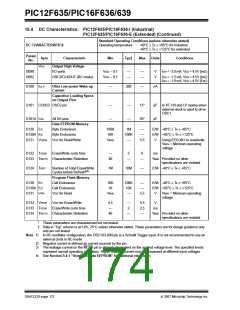
IPD
Power-down Base Current(4)
WDT, BOR, Comparators,
VREF and T1OSC disabled
(excludes AFE)
D021
IWDT
—
—
—
—
—
—
—
—
—
—
—
—
—
1.2
2.0
42
22
25
32
60
30
45
39
59
4.5
5.0
2.2
4.0
60
28
35
45
78
36
55
47
72
7.0
8.0
μA
μA
μA
μA
μA
μA
μA
μA
μA
μA
μA
μA
μA
2.0
3.0
3.0
2.0
3.0
2.0
3.0
2.0
3.0
2.0
3.0
2.0
3.0
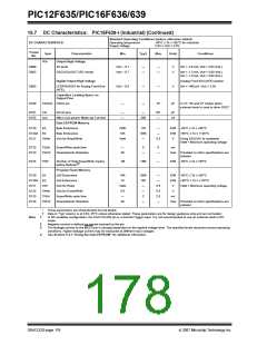
WDT Current(1)
D022A
D022B
IBOR
ILVD
BOR Current(1)
PLVD Current
D023
ICMP
Comparator Current(1)
D024A
D024B
D025
IVREFHS
IVREFLS
IT1OSC
IACT
CVREF Current(1)
(high-range)
CVREF Current(1)
(low-range)
T1OSC Current(1)
D026
Active Current of AFE only
(receiving signal)
CS = VDD; Input = Continuous
Wave (CW);
1 LC Input Channel Signal
3 LC Input Channel Signals
—
—
10
13
—
18
μA
μA
3.6
3.6
Amplitude = 300 mVPP.
All channels enabled.
D027
ISTDBY
Standby Current of AFE only
(not receiving signal)
1 LC Input Channel Enabled
CS = VDD; ALERT = VDD
—
—
—
3
4
5
5
6
7
μΑ
μA
μA
3.6
3.6
3.6
2 LC Input Channels Enabled
3 LC Input Channels Enabled
D028
ISLEEP
Sleep Current of AFE only
—
0.2
1
μA
3.6
CS = VDD; ALERT = VDD
†
Data in “Typ” column is at 3.0V, 25°C unless otherwise stated. These parameters are for design guidance only and are not tested.
The test conditions for all IDD measurements in active operation mode are: OSC1 = external square wave, from rail-to-rail; all I/O pins
tri-stated, pulled to VDD; MCLR = VDD; WDT disabled. MCU only, Analog Front-End not included.
The supply current is mainly a function of the operating voltage and frequency. Other factors, such as I/O pin loading and switching rate,
oscillator type, internal code execution pattern and temperature, also have an impact on the current consumption. MCU only, Analog
Front-End not included.
Note 1:
2:
3:
4:
The peripheral current is the sum of the base IDD or IPD and the additional current consumed when this peripheral is enabled. The
peripheral Δ current can be determined by subtracting the base IDD or IPD current from this limit. Max values should be used when
calculating total current consumption.
The power-down current in Sleep mode does not depend on the oscillator type. Power-down current is measured with the part in Sleep
mode, with all I/O pins in high-impedance state and tied to VDD.
DS41232D-page 174
© 2007 Microchip Technology Inc.

 MICROCHIP [ MICROCHIP ]