PIC12F609/615/12HV609/615
2.2.2.4
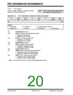
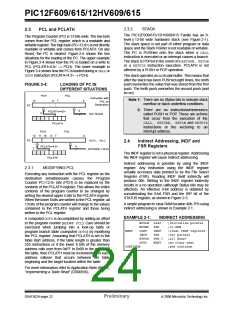
PIE1 Register
The PIE1 register contains the Peripheral Interrupt
Enable bits, as shown in Register 2-4.
Note:
Bit PEIE of the INTCON register must be
set to enable any peripheral interrupt.
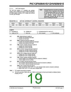
REGISTER 2-4:
PIE1: PERIPHERAL INTERRUPT ENABLE REGISTER 1
U-0
—
R/W-0
ADIE(1)
R/W-0
CCP1IE(1)
U-0
—
R/W-0
CMIE
U-0
—
R/W-0
TMR2IE(1)
R/W-0
TMR1IE
bit 7
bit 0
Legend:
R = Readable bit
-n = Value at POR
W = Writable bit
‘1’ = Bit is set
U = Unimplemented bit, read as ‘0’
‘0’ = Bit is cleared x = Bit is unknown
bit 7
bit 6
Unimplemented: Read as ‘0’
ADIE: A/D Converter (ADC) Interrupt Enable bit(1)
1= Enables the ADC interrupt
0= Disables the ADC interrupt
bit 5
CCP1IE: CCP1 Interrupt Enable bit(1)
1= Enables the CCP1 interrupt
0= Disables the CCP1 interrupt
bit 4
bit 3
Unimplemented: Read as ‘0’
CMIE: Comparator Interrupt Enable bit
1= Enables the Comparator interrupt
0= Disables the Comparator interrupt
bit 2
bit 1
Unimplemented: Read as ‘0’
TMR2IE: Timer2 to PR2 Match Interrupt Enable bit(1)
1= Enables the Timer2 to PR2 match interrupt
0= Disables the Timer2 to PR2 match interrupt
bit 0
TMR1IE: Timer1 Overflow Interrupt Enable bit
1= Enables the Timer1 overflow interrupt
0= Disables the Timer1 overflow interrupt
Note 1: PIC12F615/HV615 only. PIC12F609/HV609 unimplemented, read as ‘0’.
DS41302A-page 18
Preliminary
© 2006 Microchip Technology Inc.

 MICROCHIP [ MICROCHIP ]