PIC12F609/615/12HV609/615
2.2.2.7
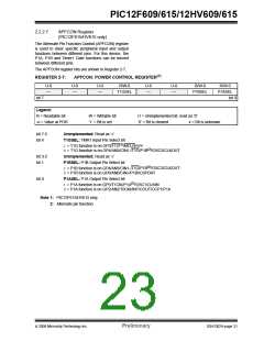
APFCON Register
(PIC12F615/HV615 only)
The Alternate Pin Function Control (APFCON) register
is used to steer specific peripheral input and output
functions between different pins. For this device, the
P1A, P1B and Timer1 Gate functions can be moved
between different pins.
The APFCON register bits are shown in Register 2-7.
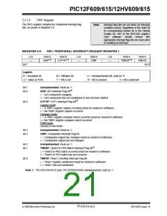
REGISTER 2-7:
APFCON: POWER CONTROL REGISTER(1)
U-0
—
U-0
—
U-0
—
R/W-0
U-0
—
U-0
—
R/W-0
R/W-0
T1GSEL
P1BSEL
P1ASEL
bit 7
bit 0
Legend:
R = Readable bit
-n = Value at POR
W = Writable bit
‘1’ = Bit is set
U = Unimplemented bit, read as ‘0’
‘0’ = Bit is cleared x = Bit is unknown
bit 7-5
bit 4
Unimplemented: Read as ‘0’
T1GSEL: TMR1 Input Pin Select bit
1= T1G function is on GP3/T1G(2)/MCLR/VPP
0= T1G function is on GP4/AN3/CIN1-/T1G/P1B(2)/OSC2/CLKOUT
bit 3-2
bit 1
Unimplemented: Read as ‘0’
P1BSEL: P1B Output Pin Select bit
1= P1B function is on GP4/AN3/CIN1-/T1G/P1B(2)/OSC2/CLKOUT
0= P1B function is on GP0/AN0/CIN+/P1B/ICSPDAT
bit 0
P1ASEL: P1A Output Pin Select bit
1= P1A function is on GP5/T1CKI/P1A(2)/OSC1/CLKIN
0= P1A function is on GP2/AN2/T0CKI/INT/COUT/CCP1/P1A
Note 1: PIC12F615/HV615 only.
2: Alternate pin function.
© 2006 Microchip Technology Inc.
Preliminary
DS41302A-page 21

 MICROCHIP [ MICROCHIP ]