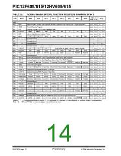
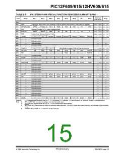
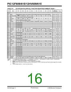
PIC12F609/615/12HV609/615
2.2.2.2
OPTION Register
Note:
To achieve a 1:1 prescaler assignment for
Timer0, assign the prescaler to the WDT
by setting PSA bit to ‘1’ of the OPTION
register. See Section 5.1.3 “Software
Programmable Prescaler”.
The OPTION register is a readable and writable regis-
ter, which contains various control bits to configure:
• Timer0/WDT prescaler
• External GP2/INT interrupt
• Timer0
• Weak pull-ups on GPIO
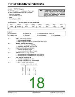
REGISTER 2-2:
OPTION_REG: OPTION REGISTER
R/W-1
GPPU
bit 7
R/W-1
R/W-1
T0CS
R/W-1
T0SE
R/W-1
PSA
R/W-1
PS2
R/W-1
PS1
R/W-1
PS0
INTEDG
bit 0
Legend:
R = Readable bit
-n = Value at POR
W = Writable bit
‘1’ = Bit is set
U = Unimplemented bit, read as ‘0’
‘0’ = Bit is cleared x = Bit is unknown
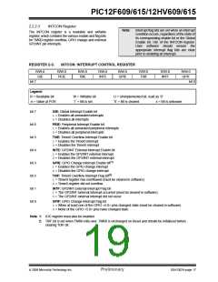
bit 7
bit 6
bit 5
bit 4
bit 3
bit 2-0
GPPU: GPIO Pull-up Enable bit
1= GPIO pull-ups are disabled
0= GPIO pull-ups are enabled by individual PORT latch values
INTEDG: Interrupt Edge Select bit
1= Interrupt on rising edge of GP2/INT pin
0= Interrupt on falling edge of GP2/INT pin
T0CS: Timer0 Clock Source Select bit
1= Transition on GP2/T0CKI pin
0= Internal instruction cycle clock (FOSC/4)
T0SE: Timer0 Source Edge Select bit
1= Increment on high-to-low transition on GP2/T0CKI pin
0= Increment on low-to-high transition on GP2/T0CKI pin
PSA: Prescaler Assignment bit
1= Prescaler is assigned to the WDT
0= Prescaler is assigned to the Timer0 module
PS<2:0>: Prescaler Rate Select bits
BIT VALUE TIMER0 RATE WDT RATE
000
001
010
011
100
101
110
111
1 : 2
1 : 4
1 : 1
1 : 2
1 : 8
1 : 4
1 : 16
1 : 32
1 : 64
1 : 128
1 : 256
1 : 8
1 : 16
1 : 32
1 : 64
1 : 128
DS41302A-page 16
Preliminary
© 2006 Microchip Technology Inc.

 MICROCHIP [ MICROCHIP ]