PIC12F609/615/12HV609/615
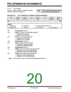
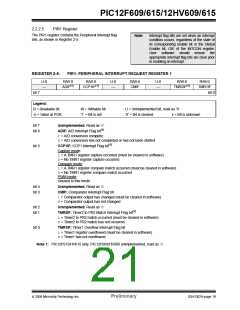
2.3.2
STACK
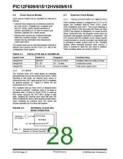
2.3
PCL and PCLATH
The PIC12F609/615/12HV609/615 Family has an 8-
level x 13-bit wide hardware stack (see Figure 2-1).
The stack space is not part of either program or data
space and the Stack Pointer is not readable or writable.
The PC is PUSHed onto the stack when a CALL
instruction is executed or an interrupt causes a branch.
The stack is POPed in the event of a RETURN, RETLW
or a RETFIE instruction execution. PCLATH is not
affected by a PUSH or POP operation.
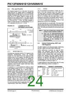
The Program Counter (PC) is 13 bits wide. The low byte
comes from the PCL register, which is a readable and
writable register. The high byte (PC<12:8>) is not directly
readable or writable and comes from PCLATH. On any
Reset, the PC is cleared. Figure 2-4 shows the two
situations for the loading of the PC. The upper example
in Figure 2-4 shows how the PC is loaded on a write to
PCL (PCLATH<4:0> → PCH). The lower example in
Figure 2-4 shows how the PC is loaded during a CALLor
GOTOinstruction (PCLATH<4:3> → PCH).
The stack operates as a circular buffer. This means that
after the stack has been PUSHed eight times, the ninth
push overwrites the value that was stored from the first
push. The tenth push overwrites the second push (and
so on).
FIGURE 2-4:
LOADING OF PC IN
DIFFERENT SITUATIONS
PCH
PCL
Instruction with
Note 1: There are no Status bits to indicate stack
12
8
7
0
PCL as
overflow or stack underflow conditions.
Destination
PC
2: There are no instructions/mnemonics
called PUSH or POP. These are actions
that occur from the execution of the
CALL, RETURN, RETLW and RETFIE
instructions or the vectoring to an
interrupt address.
8
PCLATH<4:0>
PCLATH
5
ALU Result
PCH
12 11 10
PC
PCL
8
7
0
GOTO, CALL
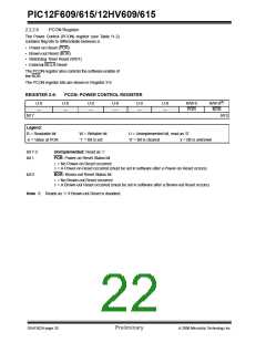
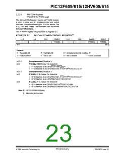
2.4
Indirect Addressing, INDF and
FSR Registers
PCLATH<4:3>
PCLATH
11
2
OPCODE <10:0>
The INDF register is not a physical register. Addressing
the INDF register will cause indirect addressing.
Indirect addressing is possible by using the INDF
register. Any instruction using the INDF register
actually accesses data pointed to by the File Select
Register (FSR). Reading INDF itself indirectly will
produce 00h. Writing to the INDF register indirectly
results in a no operation (although Status bits may be
affected). An effective 9-bit address is obtained by
concatenating the 8-bit FSR and the IRP bit of the
STATUS register, as shown in Figure 2-5.
2.3.1
MODIFYING PCL
Executing any instruction with the PCL register as the
destination simultaneously causes the Program
Counter PC<12:8> bits (PCH) to be replaced by the
contents of the PCLATH register. This allows the entire
contents of the program counter to be changed by
writing the desired upper 5 bits to the PCLATH register.
When the lower 8 bits are written to the PCL register, all
13 bits of the program counter will change to the values
contained in the PCLATH register and those being
written to the PCL register.
A simple program to clear RAM location 40h-7Fh using
indirect addressing is shown in Example 2-1.
EXAMPLE 2-1:
INDIRECT ADDRESSING
A computed GOTOis accomplished by adding an offset
to the program counter (ADDWF PCL). Care should be
exercised when jumping into a look-up table or
program branch table (computed GOTO) by modifying
the PCL register. Assuming that PCLATH is set to the
table start address, if the table length is greater than
255 instructions or if the lower 8 bits of the memory
address rolls over from 0xFF to 0x00 in the middle of
the table, then PCLATH must be incremented for each
address rollover that occurs between the table
beginning and the target location within the table.
MOVLW
MOVWF
0x40
FSR
;initialize pointer
;to RAM
NEXT
CLRF
INCF
BTFSS
GOTO
INDF
FSR
;clear INDF register
;inc pointer
FSR,7
NEXT
;all done?
;no clear next
;yes continue
CONTINUE
For more information refer to Application Note AN556,
“Implementing a Table Read” (DS00556).
DS41302A-page 22
Preliminary
© 2006 Microchip Technology Inc.

 MICROCHIP [ MICROCHIP ]