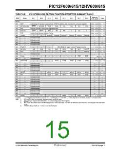
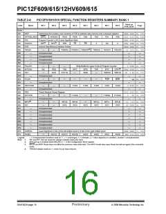
PIC12F609/615/12HV609/615
2.2.2.3
INTCON Register
Note:
Interrupt flag bits are set when an interrupt
condition occurs, regardless of the state of
its corresponding enable bit or the Global
Enable bit, GIE of the INTCON register.
User software should ensure the
appropriate interrupt flag bits are clear
prior to enabling an interrupt.
The INTCON register is a readable and writable
register, which contains the various enable and flag bits
for TMR0 register overflow, GPIO change and external
GP2/INT pin interrupts.
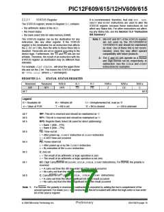
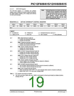
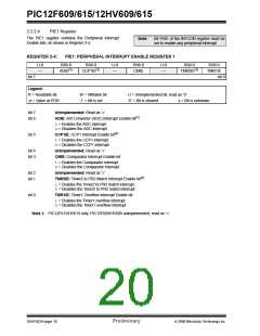
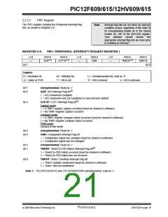
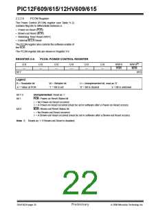
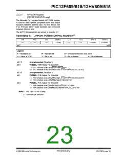
REGISTER 2-3:
INTCON: INTERRUPT CONTROL REGISTER
R/W-0
GIE
R/W-0
PEIE
R/W-0
T0IE
R/W-0
INTE
R/W-0
GPIE
R/W-0
T0IF
R/W-0
INTF
R/W-0
GPIF
bit 7
bit 0
Legend:
R = Readable bit
-n = Value at POR
W = Writable bit
‘1’ = Bit is set
U = Unimplemented bit, read as ‘0’
‘0’ = Bit is cleared x = Bit is unknown
bit 7
bit 6
bit 5
bit 4
bit 3
bit 2
bit 1
bit 0
GIE: Global Interrupt Enable bit
1= Enables all unmasked interrupts
0= Disables all interrupts
PEIE: Peripheral Interrupt Enable bit
1= Enables all unmasked peripheral interrupts
0= Disables all peripheral interrupts
T0IE: Timer0 Overflow Interrupt Enable bit
1= Enables the Timer0 interrupt
0= Disables the Timer0 interrupt
INTE: GP2/INT External Interrupt Enable bit
1= Enables the GP2/INT external interrupt
0= Disables the GP2/INT external interrupt
GPIE: GPIO Change Interrupt Enable bit(1)
1= Enables the GPIO change interrupt
0= Disables the GPIO change interrupt
T0IF: Timer0 Overflow Interrupt Flag bit(2)
1= Timer0 register has overflowed (must be cleared in software)
0= Timer0 register did not overflow
INTF: GP2/INT External Interrupt Flag bit
1= The GP2/INT external interrupt occurred (must be cleared in software)
0= The GP2/INT external interrupt did not occur
GPIF: GPIO Change Interrupt Flag bit
1= When at least one of the GPIO <5:0> pins changed state (must be cleared in software)
0= None of the GPIO <5:0> pins have changed state
Note 1: IOC register must also be enabled.
2: T0IF bit is set when TMR0 rolls over. TMR0 is unchanged on Reset and should be initialized before
clearing T0IF bit.
© 2006 Microchip Technology Inc.
Preliminary
DS41302A-page 17

 MICROCHIP [ MICROCHIP ]