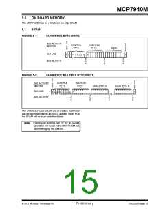
MCP7940M
• ALMxC2:0: These Configuration bits determine
the alarm match. The logic will trigger the alarm
based on one of the following match conditions:
4.2
FEATURES
4.2.1
CALIBRATION
The MCP7940M utilizes digital calibration to correct for
inaccuracies of the input clock source (either external
or crystal). Calibration is enabled by setting the value
of the Calibration register at address 08H. Calibration
is achieved by adding or subtracting a number of input
clock cycles per minute in order to achieve ppm level
adjustments in the internal timing function of the
MCP7940M.
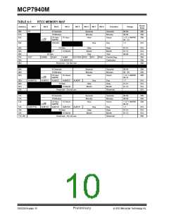
000
001
010
–
–
–
Seconds match
Minutes match
Hours match (takes into account 12/24
hour)
011
–
Matches the current day, interrupt at
12.00.00 a.m. Example: 12 midnight on
100 – Date
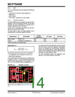
The MSB of the Calibration register is the sign bit, with
a ‘1’ indicating subtraction and a ‘0’ indicating addition.
The remaining seven bits in the register indicate the
number of input clock cycles (multiplied by two) that
are subtracted or added per minute to the internal
timing function.
101 – RESERVED
110 – RESERVED
111 – Seconds, Minutes, Hour, Day, Date,
Month
• The 12/24-hour bits 0xCh.6 and 0x13h.6 are cop-
ies of the bit in 0x02h.6. The bits are read-only.
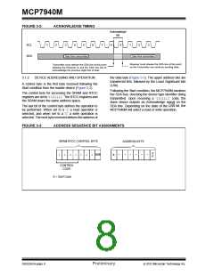
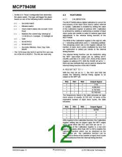
The internal timing function can be monitored using
the MFP open-drain output pin by setting bit<6>
(SQWE) and bits<2:0> (RS2, RS1, RS0) of the control
register at address 07H. With the SQWE bit set to ‘1’,
there are two methods that can be used to observe the
internal timing function of the MCP7940M:
A. RS2 BIT SET TO ‘0’
With the RS2 bit set to ‘0’, the RS1 and RS0 bits
enable the following internal timing signals to be
output on the MFP pin:
RS2
RS1
RS0
Output Signal
0
0
0
0
0
0
1
1
0
1
0
1
1 Hz
4.096 kHz
8.192 kHz
32.768 kHz
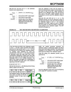
The frequencies listed in the table presume an input
clock source of exactly 32.768 kHz. In terms of the
equivalent number of input clock cycles, the table
becomes:
RS2
RS1
RS0
Output Signal
0
0
0
0
0
0
1
1
0
1
0
1
32768
8
4
1
With regards to the calibration function, the Calibration
register setting has no impact upon the MFP output
clock signal when bits RS1 and RS0 are set to ‘11’.
The setting of the Calibration register to a non-zero
value (i.e., values other than 00H or 80H) enables the
calibration function which can be observed on the
MFP output pin. The calibration function can be
expressed in terms of the number of input clock cycles
added/subtracted from the internal timing function.
DS22292A-page 12
Preliminary
2012 Microchip Technology Inc.

 MICROCHIP [ MICROCHIP ]