MCP7940M
Pointer of the MCP7940M. After receiving another
Acknowledge signal from the MCP7940M, the master
device transmits the data word to be written into the
addressed memory location. The MCP7940M
acknowledges again and the master generates a Stop
condition. After a Byte Write command, the internal
address counter will point to the address location
following the one that was just written.
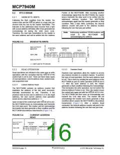
5.2
RTCC/SRAM
5.2.1
SRAM BYTE WRITE
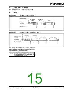
Following the Start condition from the master, the
control code and the R/W bit (which is a logic low) are
clocked onto the bus by the master transmitter. This
indicates to the addressed slave receiver that a byte
with a word address will follow after it has generated an
Acknowledge bit during the ninth clock cycle.
Therefore, the next byte transmitted by the master is
the word address and will be written into the Address
Note: Addressing undefined SRAM locations will
result
in
the
MCP7940M
not
acknowledging the address.
FIGURE 5-3:
SRAM BYTE WRITE
S
BUS ACTIVITY
T
S
T
O
P
CONTROL
BYTE
ADDRESS
BYTE
MASTER
A
R
T
DATA
SDA LINE
S 1 1 0 1 1 1 1 0
x
P
A
C
K
A
C
K
A
C
K
BUS ACTIVITY
x = don’t care for 1K devices
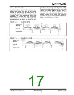
5.2.2.2
Random Read
5.2.2
READ OPERATION
Read operations are initiated in the same way as write
operations with the exception that the R/W bit of the
control byte is set to one. There are three basic types
of read operations: current address read, random read,
and sequential read.
Random read operations allow the master to access
any memory location in a random manner. To perform
this type of read operation, first the word address must
be set. This is done by sending the word address to the
MCP7940M as part of a write operation (R/W bit set to
‘0’). After the word address is sent, the master
generates a Start condition following the Acknowledge.
This terminates the write operation, but not before the
internal Address Pointer is set. Then, the master issues
the control byte again but with the R/W bit set to a one.
The MCP7940M will then issue an Acknowledge and
transmit the 8-bit data word. The master will not
acknowledge the transfer but it does generate a Stop
condition which causes the MCP7940M to discontinue
5.2.2.1
Current Address Read
The MCP7940M contains an address counter that
maintains the address of the last word accessed,
internally incremented by one. Therefore, if the
previous read access was to address n (n is any legal
address), the next current address read operation
would access data from address n + 1.
Upon receipt of the control byte with R/W bit set to one,
the MCP7940M issues an Acknowledge and transmits
the 8-bit data word. The master will not acknowledge
the transfer but does generate a Stop condition and the
MCP7940M discontinues transmission (Figure 5-4).
transmission (Figure 5-5). After
a random Read
command, the internal address counter will point to the
address location following the one that was just read.
FIGURE 5-4:
CURRENT ADDRESS
READ
S
T
A
R
T
S
T
O
P
BUS ACTIVITY
MASTER
CONTROL
BYTE
DATA
BYTE
SDA LINE
S 1 1 0 1
1
P
1 1 1
A
C
K
N
O
BUS ACTIVITY
A
C
K
DS22292A-page 16
Preliminary
2012 Microchip Technology Inc.

 MICROCHIP [ MICROCHIP ]