MCP7940M
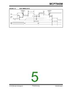
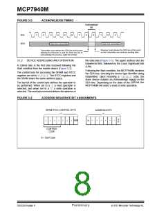
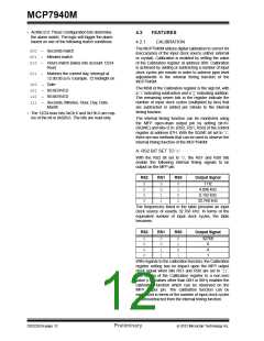
FIGURE 3-2:
ACKNOWLEDGE TIMING
Acknowledge
Bit
1
2
3
4
5
6
7
8
9
1
2
3
SCL
SDA
Data from transmitter
Data from transmitter
Receiver must release the SDA line at this point
so the Transmitter can continue sending data.
Transmitter must release the SDA line at this point
allowing the Receiver to pull the SDA line low to
acknowledge the previous eight bits of data.
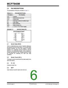
3.1.2
DEVICE ADDRESSING AND OPERATION
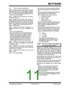
the data byte (Figure 3-3). The upper address bits are
transferred first, followed by the Least Significant bits
(LSb).
A control byte is the first byte received following the
Start condition from the master device (Figure 3-2).
Following the Start condition, the MCP7940M monitors
the SDA bus, checking the device type identifier being
transmitted. Upon receiving a ‘1101111’ code, the
slave device outputs an Acknowledge signal on the
SDA line. Depending on the state of the R/W bit, the
MCP7940M will select a read or write operation.
The control byte for accessing the SRAM and RTCC
registers are set to ‘1101111’. The RTCC registers and
the SRAM share the same address space.
The last bit of the control byte defines the operation to
be performed. When set to a ‘1’ a read operation is
selected, and when set to a ‘0’ a write operation is
selected. The next byte received defines the address of
FIGURE 3-3:
ADDRESS SEQUENCE BIT ASSIGNMENTS
SRAM RTCC CONTROL BYTE
ADDRESS BYTE
A
0
1
1
0
1
1
1
1
R/W
•
•
•
•
•
•
X
CONTROL
CODE
X = Don’t Care
DS22292A-page 8
Preliminary
2012 Microchip Technology Inc.

 MICROCHIP [ MICROCHIP ]