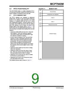
MCP7940M
With bits RS1 and RS0 set to ‘00’, the calibration
function can be expressed as:
Since the calibration is done once per minute (i.e.,
when the internal minute counter is incremented), only
one cycle in sixty of the MFP output waveform is
affected by the calibration setting. Also note that the
duty cycle of the MFP output waveform will not
necessarily be at 50% when the calibration setting is
applied.
Toutput
where:
Toutput
Tinput
=
(32768 +/- (2 * CALREG)) Tinput
=
=
=
clock period of MFP output signal
clock period of input signal
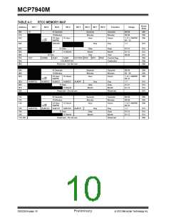
With bits RS1 and RS0 set to ‘01’ or ‘10’, the
calibration function can not be expressed in terms of
the input clock period. In the case where the MSB of
the Calibration register is set to ‘0’, the waveform
appearing at the MFP output pin will be “delayed”,
once per minute, by twice the number of input clock
cycles defined in the Calibration register. The MFP
waveform will appear as:
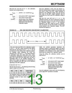
CALREG
decimal value of the Calibration
register setting and the sign is
determined by the MSB of the
Calibration register.
FIGURE 4-2:
RS1 AND RS0 WITH AND WITHOUT CALIBRATION
Delay
In the case where the MSB of the Calibration register
is set to ‘1’, the MFP output waveforms that appear
when bits RS1 and RS0 are set to ‘01’ or ‘10’ are not
as responsive to the setting of the Calibration register.
For example, when outputting the 4.096 kHz
waveform (RS1, RS0 set to ‘01’), the output waveform
is generated using only eight input clock cycles.
Consequently, attempting to subtract more than eight
input clock cycles from this output does not have a
meaningful effect on the resulting waveform. Any
effect on the output will appear as a modification in
both the frequency and duty cycle of the waveform
appearing on the MFP output pin.
Unlike the method previously described, the
calibration setting is continuously applied and affects
every cycle of the output waveform. This results in the
modulation of the frequency of the output waveform
based upon the setting of the Calibration register.
Using this setting, the calibration function can be
expressed as:
Toutput
where:
Toutput
Tinput
=
(2 * (256 +/- (2 * CALREG))) Tinput
=
=
=
clock period of MFP output signal
clock period of input signal
CALREG
decimal value of the Calibration
register setting, and the sign is
determined by the MSB of the
Calibration register.
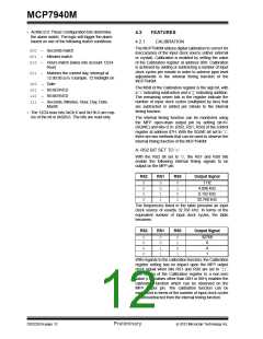
B.RS2 BIT SET TO ‘1’
With the RS2 bit set to ‘1’, the following internal timing
signal is output on the MFP pin:
Since the calibration is done every cycle, the frequency
of the output MFP waveform is constant.
RS2
RS1
RS0
Output Signal
1
x
x
64.0 Hz
The frequency listed in the table presumes an input
clock source of exactly 32.768 kHz. In terms of the
equivalent number of input clock cycles, the table
becomes:
RS2
RS1
RS0
Output Signal
1
x
x
512
2012 Microchip Technology Inc.
Preliminary
DS22292A-page 13

 MICROCHIP [ MICROCHIP ]