MCP7940M
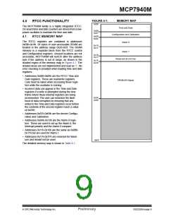
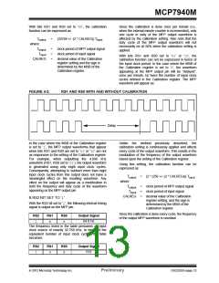
FIGURE 4-1:
0x00
MEMORY MAP
4.0
RTCC FUNCTIONALITY
The MCP7940M family is a highly integrated RTCC.
On-board time and date counters are driven from a low-
power oscillator to maintain the time and date.
Time and Date
0x06
0x07
Configuration and Calibration
0x09
0x0A
4.1
RTCC MEMORY MAP
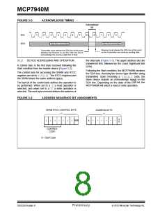
The RTCC registers are contained in addresses
0x00h-0x1fh. 64 bytes of user-accessable SRAM are
located in the address range 0x20-0x5f. The SRAM
memory is a separate block from the RTCC control
and Configuration registers. Unused locations are not
accessible, MCP7940M will noACK after the address
byte if the address is out of range, as shown in the
shaded region of the memory map in Figure 4-1. The
shaded areas are not implemented and read as ‘0’. No
error checking is provided when loading time and date
registers.
Alarm 0
0x10
0x11
Alarm 1
0x16
0x17
Reserved do not Use
0x1F
0x20
• Addresses 0x00h-0x06h are the RTCC Time and
Date registers. These are read/write registers.
Care must be taken when accessing these regis-
ters while the oscillator is running.
SRAM (64 Bytes)
• Incorrect data can appear in the Time and Date
registers if a write is attempted during the time
frame where these internal registers are being
incremented. The user can minimize the likeli-
hood of data corruption by ensuring that any
writes to the Time and Date registers occur before
the contents of the second register reach a value
of 0x59H.
0x5F
0x60
• Addresses 0x07h-0x09h are the device Configu-
ration and Calibration.
• Addresses 0x0Ah-0x10h are the Alarm 0 regis-
ters. These are used to set up the Alarm 0, the
Interrupt polarity and the Alarm 0 compare.
• Addresses 0x11h-0x16h are the same as 0x0Bh-
0x11h but are used for Alarm 1.
• Addresses 0x17h-0x1Fh are reserved for future
use and should not be used.
0xFF
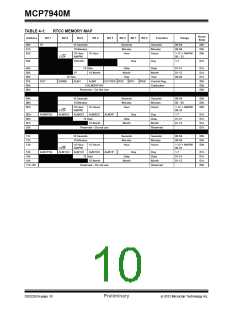
The detailed memory map is shown in Table 4-1.
2012 Microchip Technology Inc.
Preliminary
DS22292A-page 9

 MICROCHIP [ MICROCHIP ]