MCP6271/1R/2/3/4/5
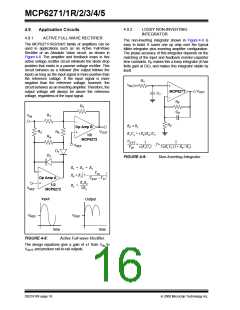
4.9.2
LOSSY NON-INVERTING
INTEGRATOR
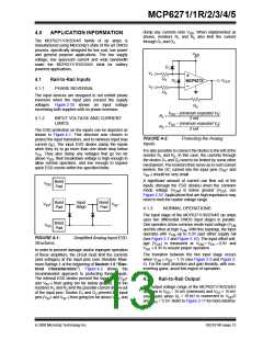
4.9
Application Circuits
4.9.1
ACTIVE FULL-WAVE RECTIFIER
The non-inverting integrator shown in Figure 4-9 is
easy to build. It saves one op amp over the typical
Miller integrator plus inverting amplifier configuration.
The phase accuracy of this integrator depends on the
matching of the input and feedback resistor-capacitor
time constants. RF makes this a lossy integrator (it has
finite gain at DC), and makes this integrator stable by
itself.
The MCP6271/1R/2/3/4/5 family of amplifiers can be
used in applications such as an Active Full-Wave
Rectifier or an Absolute Value circuit, as shown in
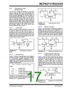
Figure 4-8. The amplifier and feedback loops in this
active voltage rectifier circuit eliminate the diode drop
problem that exists in a passive voltage rectifier. This
circuit behaves as a follower (the output follows the
input) as long as the input signal is more positive than
the reference voltage. If the input signal is more
negative than the reference voltage, however, the
circuit behaves as an inverting amplifier. Therefore, the
output voltage will always be above the reference
voltage, regardless of the input signal.
R1
VIN
+
VOUT
MCP6271
_
C1
RF
C2
R2
R1
VIN
–
R2
RF ≈ R2
Op Amp B
R3
VOUT
R5
+
R1C1 = (R2||RF)C2
1/2
MCP6272
R4
D2
VOUT
------------- --------------------
1
1
---------------------------------------------------
≈
,
f ≈
VREF
VIN
s(R1C1)
2πR1C1(1 + RF ⁄ R2)
D1
FIGURE 4-9:
Non-Inverting Integrator.
R1 = R2 = R3
–
VD1
⎛
⎞
⎠
R4 < R3 1 –
---------------------------
⎝
VREF – VSS
Op Amp A
R2R4
R5 = ------------
2R3
+
1/2
MCP6272
VREF
Input
Output
VREF
VREF
time
time
FIGURE 4-8:
Active Full-wave Rectifier.
The design equations give a gain of ±1 from VIN to
VOUT, and produce rail-to-rail outputs.
DS21810F-page 16
© 2008 Microchip Technology Inc.

 MICROCHIP [ MICROCHIP ]