MCP6271/1R/2/3/4/5
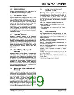
4.9.3
CASCADED OP AMP
APPLICATIONS
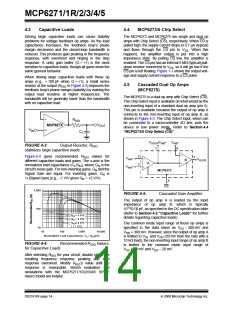
R4
R3
R2
R1
The MCP6275 provides the flexibility of Low power
mode for dual op amps in an 8-pin package. The
MCP6275 eliminates the added cost and space in a
battery powered application by using two single op
amps with Chip Select (CS) lines or a 10-pin device
with one CS line for both op amps. Since the two op
amps are internally cascaded, this device cannot be
used in circuits that require active or passive elements
between the two op amps. However, there are several
applications where this op amp configuration with a CS
line becomes suitable. The circuits below show
possible applications for this device.
VOUT
B
A
VIN
MCP6275
CS
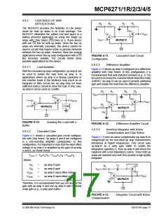
FIGURE 4-11:
Configuration.
Cascaded Gain Circuit
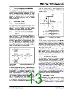
4.9.3.3
Difference Amplifier
4.9.3.1
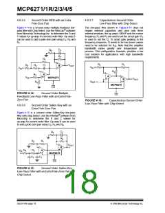
Load Isolation
Figure 4-12 shows op amp A configured as a difference
amplifier with Chip Select. In this configuration, it is
recommended that well matched resistors (e.g., 0.1%)
be used to increase the Common Mode Rejection Ratio
(CMRR). Op amp B can be used to provide additional
gain and isolate the load from the difference amplifier.
With the cascaded op amp configuration, op amp B can
be used to isolate the load from op amp A. In
applications where op amp A is driving capacitive or
low resistive loads in the feedback loop (such as an
integrator or filter circuit) the op amp may not have
sufficient source current to drive the load. In this case,
op amp B can be used as a buffer.
R2
R1
R4
R3
VIN2
VOUTB
B
VOUT
B
A
R2
A
Load
MCP6275
VIN1
MCP6275
R1
CS
CS
FIGURE 4-10:
Buffer.
Isolating the Load with a
FIGURE 4-12:
4.9.3.4
Difference Amplifier Circuit.
Inverting Integrator with Active
Compensation and Chip Select
4.9.3.2
Cascaded Gain
Figure 4-11 shows a cascaded gain circuit configura-
tion with Chip Select. Op amps A and B are configured
in a non-inverting amplifier configuration. In this
configuration, it is important to note that the input offset
voltage of op amp A is amplified by the gain of op amp
A and B, as shown below:
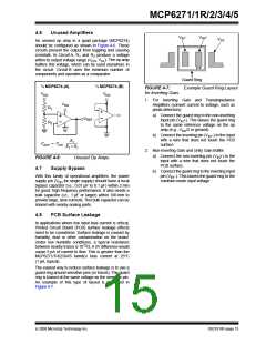
Figure 4-13 uses an active compensator (op amp B) to
compensate for the non-ideal op amp characteristics
introduced at higher frequencies. This circuit uses
op amp B as a unity gain buffer to isolate the
integration capacitor C1 from op amp A and drives the
capacitor with a low impedance source. Since both op
amps are matched very well, they provide a high quality
integrator.
VOUT = VINGAGB + VOSAGAGB + VOSBGB
Where:
GA
GB
=
=
=
=
op amp A gain
C1
R1
op amp B gain
VIN
B
VOSA
VOSB
op amp A input offset voltage
op amp B input offset voltage
VOUT
A
MCP6275
Therefore, it is recommended that you set most of the
gain with op amp A and use op amp B with relatively
small gain (e.g., a unity gain buffer).
CS
FIGURE 4-13:
Integrator Circuit with Active
Compensation.
© 2008 Microchip Technology Inc.
DS21810F-page 17

 MICROCHIP [ MICROCHIP ]