MCP6271/1R/2/3/4/5
4.3
Capacitive Loads
4.4
MCP6273/5 Chip Select
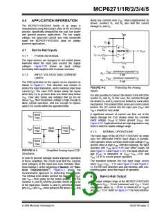
Driving large capacitive loads can cause stability
problems for voltage feedback op amps. As the load
capacitance increases, the feedback loop’s phase
margin decreases and the closed-loop bandwidth is
reduced. This produces gain peaking in the frequency
response, with overshoot and ringing in the step
response. A unity gain buffer (G = +1) is the most
sensitive to capacitive loads, though all gains show the
same general behavior.
The MCP6273 and MCP6275 are single and dual op
amps with Chip Select (CS), respectively. When CS is
pulled high, the supply current drops to 0.7 µA (typical)
and flows through the CS pin to VSS. When this
happens, the amplifier output is put into a high
impedance state. By pulling CS low, the amplifier is
enabled. The CS pin has an internal 5 MΩ (typical) pull-
down resistor connected to VSS, so it will go low if the
CS pin is left floating. Figure 1-1 shows the output volt-
age and supply current response to a CS pulse.
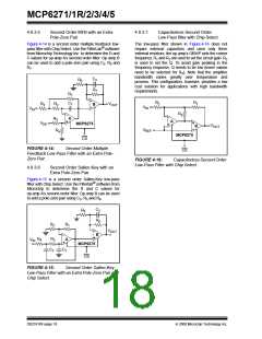
When driving large capacitive loads with these op
amps (e.g., > 100 pF when G = +1), a small series
resistor at the output (RISO in Figure 4-3) improves the
feedback loop’s phase margin (stability) by making the
output load resistive at higher frequencies. The
bandwidth will be generally lower than the bandwidth
with no capacitive load.
4.5
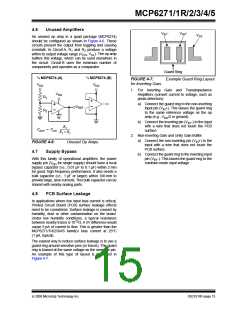
Cascaded Dual Op Amps
(MCP6275)
The MCP6275 is a dual op amp with Chip Select (CS).
The Chip Select input is available on what would be the
non-inverting input of a standard dual op amp (pin 5).
This pin is available because the output of op amp A
connects to the non-inverting input of op amp B, as
shown in Figure 4-5. The Chip Select input, which can
be connected to a microcontroller I/O line, puts the
device in low power mode. Refer to Section 4.4
“MCP6273/5 Chip Select (CS)”.
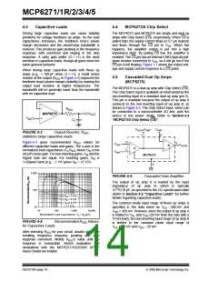
–
RISO
VOUT
MCP627X
VIN
+
CL
VINB
–
VOUTA/VINB
1
+
FIGURE 4-3:
stabilizes large capacitive loads.
Output Resistor, R
ISO
6
2
3
Figure 4-4 gives recommended RISO values for
different capacitive loads and gains. The x-axis is the
normalized load capacitance (CL/GN), where GN is the
circuit's noise gain. For non-inverting gains, GN and the
Signal Gain are equal. For inverting gains, GN is
1+|Signal Gain| (e.g., –1 V/V gives GN = +2 V/V).
7
VINA
VINA
–
VOUTB
B
A
+
MCP6275
5
CS
1,000
FIGURE 4-5:
Cascaded Gain Amplifier.
The output of op amp A is loaded by the input
impedance of op amp B, which is typically
1013Ω⎟⎟6 pF, as specified in the DC specification table
(Refer to Section 4.3 “Capacitive Loads” for further
details regarding capacitive loads).
100
GN = 1 V/V
GN = 2 V/V
GN t 4 V/V
The common mode input range of these op amps is
specified in the data sheet as VSS – 300 mV and
VDD + 300 mV. However, since the output of op amp A
is limited to VOL and VOH (20 mV from the rails with a
10 kΩ load), the non-inverting input range of op amp B
is limited to the common mode input range of
VSS + 20 mV and VDD – 20 mV.
10
10
100
1,000
10,000
Normalized Load Capacitance; CL / GN (pF)
FIGURE 4-4:
for Capacitive Loads.
Recommended R
Values
ISO
After selecting RISO for your circuit, double check the
resulting frequency response peaking and step
response overshoot. Modify RISO's value until the
response is reasonable. Bench evaluation and
simulations with the MCP6271/1R/2/3/4/5 SPICE
macro model are helpful.
DS21810F-page 14
© 2008 Microchip Technology Inc.

 MICROCHIP [ MICROCHIP ]