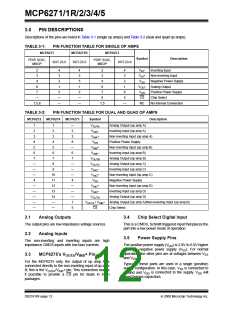
MCP6271/1R/2/3/4/5
3.0
PIN DESCRIPTIONS
Descriptions of the pins are listed in Table 3-1 (single op amps) and Table 3-2 (dual and quad op amps).
TABLE 3-1: PIN FUNCTION TABLE FOR SINGLE OP AMPS
MCP6271
MCP6271R
MCP6273
PDIP, SOIC,
Symbol
Description
PDIP, SOIC,
MSOP
SOT-23-5
SOT-23-5
SOT-23-6
MSOP
2
3
4
3
4
3
2
3
4
3
VIN
–
+
Inverting Input
VIN
Non-inverting Input
Negative Power Supply
Analog Output
4
2
5
4
2
VSS
VOUT
VDD
CS
6
1
1
6
1
7
5
2
7
6
Positive Power Supply
Chip Select
—
1,5,8
—
—
—
—
8
5
1,5
—
NC
No Internal Connection
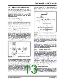
TABLE 3-2:
PIN FUNCTION TABLE FOR DUAL AND QUAD OP AMPS
MCP6272
MCP6274
MCP6275
Symbol
Description
1
2
1
2
—
2
VOUTA
Analog Output (op amp A)
Inverting Input (op amp A)
VINA
–
+
3
3
3
VINA
Non-inverting Input (op amp A)
Positive Power Supply
8
4
8
VDD
5
5
—
6
VINB
+
Non-inverting Input (op amp B)
Inverting Input (op amp B)
Analog Output (op amp B)
Analog Output (op amp C)
Inverting Input (op amp C)
Non-inverting Input (op amp C)
Negative Power Supply
6
6
VINB
–
7
7
7
VOUTB
VOUTC
—
—
—
4
8
—
—
—
4
9
VINC
–
+
10
11
12
13
14
—
—
VINC
VSS
—
—
—
—
—
—
—
—
1
VIND
+
Non-inverting Input (op amp D)
Inverting Input (op amp D)
Analog Output (op amp D)
Analog Output (op amp A)/Non-inverting Input (op amp B)
Chip Select
VIND
–
VOUTD
OUTA / VINB
CS
V
+
5
3.1
Analog Outputs
3.4
Chip Select Digital Input
The output pins are low impedance voltage sources.
This is a CMOS, Schmitt triggered input that places the
part into a low power mode of operation.
3.2
Analog Inputs
3.5
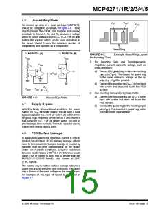
Power Supply Pins
The non-inverting and inverting inputs are high
impedance CMOS inputs with low bias currents.
The positive power supply (VDD) is 2.0V to 6.0V higher
than the negative power supply (VSS). For normal
operation, the other pins are at voltages between VSS
3.3
MCP6275’s VOUTA/VINB+ Pin
and VDD
.
For the MCP6275 only, the output of op amp A is
connected directly to the non-inverting input of op amp
B; this is the VOUTA/VINB+ pin. This connection makes
it possible to provide a CS pin for duals in 8-pin
packages.
Typically, these parts are used in a single (positive)
supply configuration. In this case, VSS is connected to
ground and VDD is connected to the supply. VDD will
need bypass capacitors.
DS21810F-page 12
© 2008 Microchip Technology Inc.

 MICROCHIP [ MICROCHIP ]