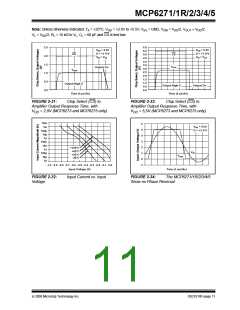
MCP6271/1R/2/3/4/5
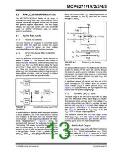
4.6
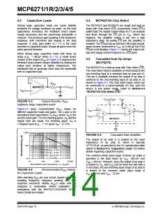
Unused Amplifiers
VIN–
VIN+
VSS
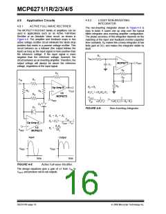
An unused op amp in a quad package (MCP6274)
should be configured as shown in Figure 4-6. These
circuits prevent the output from toggling and causing
crosstalk. In Circuit A, R1 and R2 produce a voltage
within its output voltage range (VOH, VOL). The op amp
buffers this voltage, which can be used elsewhere in
the circuit. Circuit B uses the minimum number of
components and operates as a comparator.
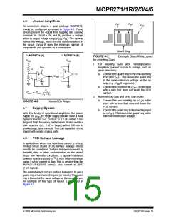
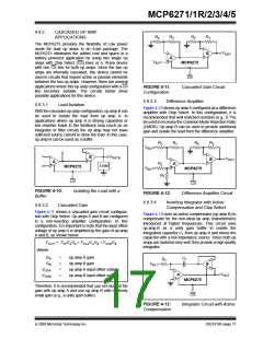
Guard Ring
Example Guard Ring Layout
¼ MCP6274 (A)
¼ MCP6274 (B)
FIGURE 4-7:
for Inverting Gain.
VDD
VDD
1. For Inverting Gain and Transimpedance
Amplifiers (convert current to voltage, such as
photo detectors):
VDD
R1
a) Connect the guard ring to the non-inverting
input pin (VIN+). This biases the guard ring
to the same reference voltage as the op
amp (e.g., VDD/2 or ground).
VREF
R2
b) Connect the inverting pin (VIN–) to the input
with a wire that does not touch the PCB
surface.
R2
------------------
⋅
VREF = VDD
R1 + R2
2. Non-inverting Gain and Unity Gain Buffer:
a) Connect the non-inverting pin (VIN+) to the
input with a wire that does not touch the
PCB surface.
FIGURE 4-6:
Unused Op Amps.
4.7
Supply Bypass
b) Connect the guard ring to the inverting input
pin (VIN–). This biases the guard ring to the
common mode input voltage.
With this family of operational amplifiers, the power
supply pin (VDD for single supply) should have a local
bypass capacitor (i.e., 0.01 µF to 0.1 µF) within 2 mm
for good, high frequency performance. It also needs a
bulk capacitor (i.e., 1 µF or larger) within 100 mm to
provide large, slow currents. This bulk capacitor can be
shared with nearby analog parts.
4.8
PCB Surface Leakage
In applications where low input bias current is critical,
Printed Circuit Board (PCB) surface leakage effects
need to be considered. Surface leakage is caused by
humidity, dust or other contamination on the board.
Under low humidity conditions, a typical resistance
between nearby traces is 1012Ω. A 5V difference would
cause 5 pA of current to flow. This is greater than the
MCP6271/1R/2/3/4/5 family’s bias current at 25°C
(1 pA, typical).
The easiest way to reduce surface leakage is to use a
guard ring around sensitive pins (or traces). The guard
ring is biased at the same voltage as the sensitive pin.
An example of this type of layout is illustrated in
Figure 4-7.
© 2008 Microchip Technology Inc.
DS21810F-page 15

 MICROCHIP [ MICROCHIP ]