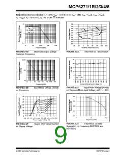
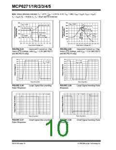
MCP6271/1R/2/3/4/5
dump any currents onto VDD. When implemented as
shown, resistors R1 and R2 also limit the current
through D1 and D2.
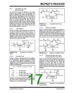
4.0
APPLICATION INFORMATION
The MCP6271/1R/2/3/4/5 family of op amps is
manufactured using Microchip’s state of the art CMOS
process, specifically designed for low cost, low power
and general purpose applications. The low supply
voltage, low quiescent current and wide bandwidth
make the MCP6271/1R/2/3/4/5 ideal for battery
powered applications.
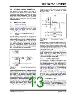
VDD
D1
R1
V1
4.1
Rail-to-Rail Inputs
D2
VOUT
MCP627X
V2
4.1.1
PHASE REVERSAL
R2
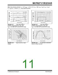
The input devices are designed to not exhibit phase
inversion when the input pins exceed the supply
voltages. Figure 2-34 shows an input voltage
exceeding both supplies with no phase inversion.
R3
VSS – (minimum expected V1)
R1 >
R2 >
4.1.2
INPUT VOLTAGE AND CURRENT
LIMITS
2 mA
VSS – (minimum expected V2)
2 mA
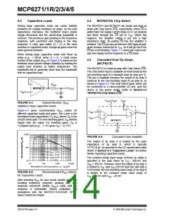
The ESD protection on the inputs can be depicted as
shown in Figure 4-1. This structure was chosen to
protect the input transistors, and to minimize input bias
current (IB). The input ESD diodes clamp the inputs
when they try to go more than one diode drop below
VSS. They also clamp any voltages that go too far
above VDD; their breakdown voltage is high enough to
allow normal operation, and low enough to bypass
quick ESD events within the specified limits.
FIGURE 4-2:
Inputs.
Protecting the Analog
It is also possible to connect the diodes to the left of the
resistor R1 and R2. In this case, the currents through
the diodes D1 and D2 need to be limited by some other
mechanism. The resistors then serve as in-rush current
limiters; the DC current into the input pins (VIN+ and
VIN–) should be very small.
A significant amount of current can flow out of the
inputs (through the ESD diodes) when the common
mode voltage (VCM) is below ground (VSS); see
Figure 2-32. Applications that are high impedance may
need to limit the usable voltage range.
Bond
VDD
Pad
Bond
Pad
Bond
Pad
Input
Stage
VIN+
VIN–
4.1.3
NORMAL OPERATIONS
The input stage of the MCP6271/1R/2/3/4/5 op amps
uses two differential CMOS input stages in parallel.
One operates at low common mode input voltage (VCM
and the other at high VCM. With this topology, the input
operates with VCM up to 0.3V past either supply rail
(see Figure 2-7 and Figure 2-10). The input offset volt-
age (VOS) is measured at VCM = VSS – 0.3V and
VDD + 0.3V to ensure proper operation.
Bond
Pad
VSS
FIGURE 4-1:
Structures.
Simplified Analog Input ESD
In order to prevent damage and/or improper operation
of these amplifiers, the circuit must limit the currents
(and voltages) at the input pins (see Absolute Maxi-
mum Ratings † at the beginning of Section 1.0 “Elec-
trical Characteristics”). Figure 4-2 shows the
recommended approach to protecting these inputs.
The internal ESD diodes prevent the input pins (VIN+
and VIN–) from going too far below ground, and the
resistors R1 and R2 limit the possible current drawn out
of the input pins. Diodes D1 and D2 prevent the input
pins (VIN+ and VIN–) from going too far above VDD, and
The transition between the two input stage occurs
when VCM ≈ VDD – 1.1V (see Figure 2-3 and Figure 2-
6). For the best distortion and gain linearity, with non-
inverting gains, avoid this region of operation.
4.2
Rail-to-Rail Output
The output voltage range of the MCP6271/1R/2/3/4/5
op amps is VDD – 15 mV (minimum) and VSS + 15 mV
(maximum) when RL = 10 kΩ is connected to VDD/2
and VDD = 5.5V. Refer to Figure 2-17 for more informa-
tion.
© 2008 Microchip Technology Inc.
DS21810F-page 13

 MICROCHIP [ MICROCHIP ]