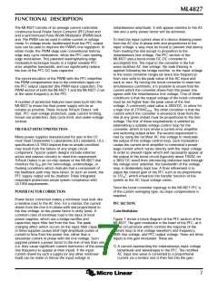
ML4827
FUNCTIONAL DESCRIPTION (Continued)
voltage for which the PWM output transistor must be
rated. Frequently, the design of the tranformer’s reset
winding, and/or of the output transistor’s snubbers or
clamps, require an additional voltage margin of 100V to
200V.
at the lowest guaranteed value for δ, to ensure that the
magnetics will deliver full output power with any
individual ML4827. In actual operation, the choice of
δ
= 60% will allow some tolerance for the timing
MIN
capacitors and resistors. A tolerance on (R
x
RAMP2
C
) of ±2% is the simplest “brute force” way to
RAMP2
achieve the desired result. This should be combined with
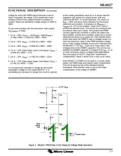
an external duty cycle clamp. This protects the PWM
circuitry against the condition in which the output has
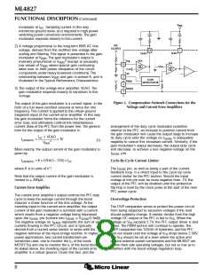
To put some numbers into the discussion, with a given
V
of 400V:
BUSS(MAX)
been shorted, and the error amplifier output (V ) would
1. For δ = 50%: V
= {[(1/f
) x δ]/[(1/f ) x
PWM
DC
RESET
PWM
otherwise be driven to its upper rail. One method which
works well when the PWM is used in voltage mode is to
limit the maximum input to the PWM feedback voltage
(1–δ)]} x 400V = 0.50/0.50 x 400V = 400V
2. For δ = 55%: V
3. For δ = 60%: V
= 0.55/0.45 x 400V = 489V
= 0.60/0.40 x 400V = 600V
RESET
(V ). If the voltage available to this pin is derived from
DC
the ML4827’s 7.5V V , it will be in close ratio to the
REF
RESET
charging time of the RAMP2 capacitor. This will be true
whether the RAMP2 capacitor is charged from V , or, as
4. For δ = 64% (Data Sheet Lower Limit Value): V
=
=
REF
RESET
is more commonly done in voltage-mode applications,
from the output of the PFC Stage (the “feedforward”
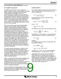
configuration). Figure 3 shows such a duty cycle clamp.
0.64/0.36 x 400V = 711V
5. For δ = 70%: V
= 0.70/0.30 x 400V = 933V
RESET
If the ML4827-2’s PWM is to be used in a current-mode
design, the PWM stage will require slope compensation.
This can be done by any of the standard industry
techniques. Note that the ramp to use for this slope
compensation is the voltage on RAMP1.
6. For δ = 74% (Data Sheet Upper Limit Value): V
RESET
0.74/0.26 x 400V = 1138V
It is economically desirable to design for the lowest
meaningful voltage on the output MOSFET. It is
simultaneously necessary to design the circuit to operate
PFC V
BUSS
R
R
FB1
FB2
R
RAMP2
V
FB
RAMP2
C
RAMP2
V
V
REF
R1
PWM
ERROR
AMP
DC
R2
R
R
V
2
1
REF
+ R
δ
=
V
RAMP2 (PEAK)
MAX
2
Figure 3. ML4827- PWM Duty Cycle Clamp for Voltage-Made Operation
11

 MICRO-LINEAR [ MICRO LINEAR CORPORATION ]