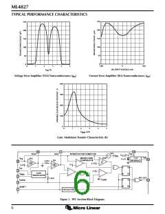
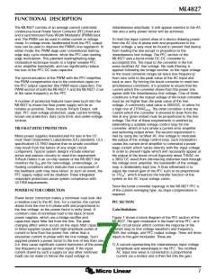
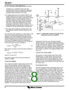
ML4827
FUNCTIONAL DESCRIPTION (Continued)
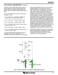
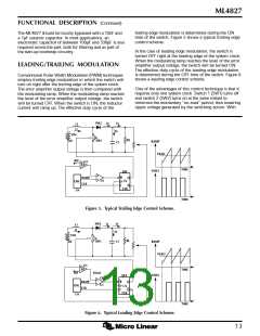
PWM SECTION
fewer turns on forward converter reset windings. Long
duty cycles, by allowing greater utilization of the PFC’s
stored charge, can also lower the cost of PFC bus
capacitors while still offering long “hold-up” times.
PulseWidth Modulator
The PWM section of the ML4827 is straightforward, but
there are several points which should be noted. Foremost
among these is its inherent synchronization to the PFC
section of the device, from which it also derives its basic
timing. The PWM is capable of current-mode or voltage
mode operation. In current-mode applications, the PWM
ramp (RAMP 2) is usually derived directly from a current
sensing resistor or current transformer in the primary of the
output stage, and is thereby representative of the current
NOTE: during the time when the PWM switch is off (the
reset or flyback periods), increasing duty cycles will result
in rapidly increasing peak voltages across the switch.
This result of high PWM duty cycles requires greater care
be used in circuit design. Relevant design issues include:
•
•
Higher voltage (>1000V) PWM switches
flowing in the converter’s output stage. DC I , which
LIMIT
More carefully designed and tested PWM
transformers
provides cycle-by-cycle current limiting, is typically
connected to RAMP 2 in such applications. For voltage-
mode operation or certain specialized applications,
RAMP 2 can be connected to a separate RC timing
network to generate a voltage ramp against which VDC
will be compared. Under these conditions, the use of
voltage feedforward from the PFC buss can assist in line
regulation accuracy and response. As in current mode
•
Clamps and/or snubbers when needed
Also, slope compensation will be required in most current
mode PWM designs.
For those who want to approach the limits of attainable
performance (most commonly high-volume, low-cost
supplies), the ML4827-2’s 70% maximum PWM duty
cycle offers several desirable design capabilities. Using a
70% duty cycle makes it essential to perform a careful
magnetics design and component stress analysis before
finalizing designs with the ML4827-2.
operation, the DC I
input would is used for output
LIMIT
stage overcurrent protection.
No voltage error amplifier is included in the PWM stage
of the ML4827, as this function is generally performed on
the output side of the PWM’s isolation boundary. To
facilitate the design of optocoupler feedback circuitry, an
offset has been built into the PWM’s RAMP 2 input which
THE ML4827-2: SPECIAL CONSIDERATIONS FOR HIGH
DUTY CYCLES
allows V to command a zero percent duty cycle for
DC
input voltages below 1.25V.
The use of the ML4827-1, especially with the type of
PWM output stage shown in the Application Circuit of
Figure 6, is straightforward due to the limitation of the
PWM duty cyle to 50% maximum. In fact, one of the
advantages of the “two-transistor single-ended forward
converter” shown in Figure 6 is that it will necessarily
reset the core, with no additional winding required, as
long as the core does not go into saturation during the
topology's maximum permissible 50% duty cycle.
Maximum Duty Cycle
In the ML4827-1, the maximum duty cycle of the PWM
section is limited to 50% for ease of use and design. In
the case of the ML4827-2, the maximum duty cycle of
the PWM section is extended to 70% (typical) for
enhanced utilization of the inductor. Operation at 70%
duty cycle requires special care in circuit design to avoid
volt-second imbalances, and/or high-voltage damage to
the PWM switch transistor(s).
For the “-2” version of the ML4827, the maximum duty
cycle (δ) of the PWM is nominally 70%. As the two-
transistor single-ended forward converter cannot be used
at duty cycles greater than 50%, high-δ applications
require the use of either a single-transistor forward
converter (with a transformer reset winding), or a flyback
output stage. In either case, special concerns arise
regarding the peak voltage appearing on the PWM switch
transistor, the PWM output transformer, and associated
power components as the duty cycle increases. For any
output stage topology, the available on-time (core “set”
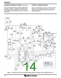
Using the ML4827-2
The ML4827-2’s higher PWM duty cycle offers several
design advantages that skilled power supply and
magnetics engineers can take advantage of, including:
•
•
Reduced RMS and peak PWM switch currents
Reduced RMS and peak PWM transformer
currents
time) is (1/f ) x δ, while the reset time for the core of
PWM
the PWM output transformer is (1/f
) x (1–δ). This
PWM
•
Easier RFI/EMI filtering due to lower peak
currents
means that the magnetizing inductance of the core
charges for a period of (1/f ) x δ, and must be
PWM
completely discharged during a period of (1/f
) x
PWM
These reduced currents can result in cost savings by
allowing smaller PWM transformer primary windings and
(1–δ). The ratio of these two periods, multiplied by the
maximum value of the PFC’s V , yields the minimum
BUSS
10

 MICRO-LINEAR [ MICRO LINEAR CORPORATION ]