ML4827
FUNCTIONAL DESCRIPTION (Continued)
V
REF
modulator at I . Sampling current in this way
AC
minimizes ground noise, as is required in high power
switching power conversion environments. The gain
modulator responds linearly to this current.
PFC
OUTPUT
2) A voltage proportional to the long-term RMS AC line
voltage, derived from the rectified line voltage after
scaling and filtering. This signal is presented to the gain
16
1
IEAO
VEAO
VEA
modulator at V
inversely proportional to V
low values of V
. The gain modulator’s output is
RMS
V
2
FB
(except at unusually
RMS
IEA
15
–
where special gain contouring
RMS
+
–
+
–
2.5V
AC
+
takes over, to limit power dissipation of the circuit
components under heavy brownout conditions). The
I
2
4
3
relationship between V
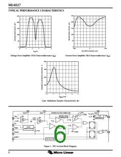
illustrated in the Typical Performance Characteristics.
and gain is termed K, and is
RMS
GAIN
MODULATOR
V
RMS
I
3) The output of the voltage error amplifier, VEAO. The
gain modulator responds linearly to variations in this
voltage.
SENSE
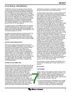
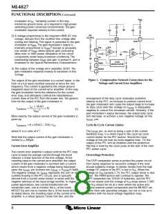
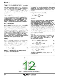
Figure 2. Compensation Network Connections for the
Voltage and Current Error Amplifiers
The output of the gain modulator is a current signal, in the
form of a full wave rectified sinusoid at twice the line
frequency. This current is applied to the virtual-ground
(negative) input of the current error amplifier. In this way
the gain modulator forms the reference for the current
error loop, and ultimately controls the instantaneous
current draw of the PFC from the power line. The general
form for the output of the gain modulator is:
arrangement of the duty cycle modulator polarities
internal to the PFC, an increase in positive current from
the gain modulator will cause the output stage to increase
IAC ´ VEAO
its duty cycle until the voltage on I
is adequately
SENSE
IGAINMOD
=
´ 1V
(1)
2
negative to cancel this increased current. Similarly, if the
gain modulator’s output decreases, the output duty cycle
will decrease, to achieve a less negative voltage on the
V
RMS
More exactly, the output current of the gain modulator is
given by:
I
pin.
SENSE
IGAINMOD = K ´ (VEAO - 1.5V) ´ IAC
Cycle-By-Cycle Current Limiter
The I pin, as well as being a part of the current
-1
where K is in units of V .
SENSE
feedback loop, is a direct input to the cycle-by-cycle
current limiter for the PFC section. Should the input
voltage at this pin ever be more negative than -1V, the
output of the PFC will be disabled until the protection
flip-flop is reset by the clock pulse at the start of the next
PFC power cycle.
Note that the output current of the gain modulator is
limited to 200µA.
Current Error Amplifier
The current error amplifier’s output controls the PFC duty
cycle to keep the average current through the boost
inductor a linear function of the line voltage. At the
inverting input to the current error amplifier, the output
current of the gain modulator is summed with a current
which results from a negative voltage being impressed
Overvoltage Protection
The OVP comparator serves to protect the power circuit
from being subjected to excessive voltages if the load
should suddenly change. A resistor divider from the high
upon the I
The negative voltage on I
pin (current into I
V
/3.5kΩ).
voltage DC output of the PFC is fed to V . When the
SENSE
SENSE
SENSE
FB
represents the sum of all
voltage on V exceeds 2.7V, the PFC output driver is shut
SENSE
FB
currents flowing in the PFC circuit, and is typically
derived from a current sense resistor in series with the
negative terminal of the input bridge rectifier. In higher
power applications, two current transformers are
down. The PWM section will continue to operate. The
OVP comparator has 125mV of hysteresis, and the PFC
will not restart until the voltage at V drops below 2.58V.
FB
The V should be set at a level where the active and
FB
sometimes used, one to monitor the I of the boost
passive external power components and the ML4827 are
within their safe operating voltages, but not so low as to
interfere with the boost voltage regulation loop.
D
MOSFET(s) and one to monitor the I of the boost diode.
F
As stated above, the inverting input of the current error
amplifier is a virtual ground. Given this fact, and the
8

 MICRO-LINEAR [ MICRO LINEAR CORPORATION ]