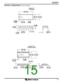
ML4827
FUNCTIONAL DESCRIPTION (Continued)
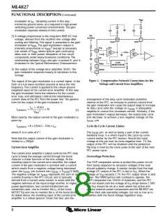
trailing edge modulation is determined during the ON
time of the switch. Figure 5 shows a typical trailing edge
control scheme.
The ML4827 should be locally bypassed with a 10nF and
a 1µF ceramic capacitor. In most applications, an
electrolytic capacitor of between 100µF and 330µF is also
required across the part, both for filtering and as part of
the start-up bootstrap circuitry.
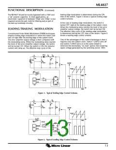
In the case of leading edge modulation, the switch is
turned OFF right at the leading edge of the system clock.
When the modulating ramp reaches the level of the error
amplifier output voltage, the switch will be turned ON.
The effective duty-cycle of the leading edge modulation
is determined during the OFF time of the switch. Figure 6
shows a leading edge control scheme.
LEADING/TRAILING MODULATION
Conventional Pulse Width Modulation (PWM) techniques
employ trailing edge modulation in which the switch will
turn on right after the trailing edge of the system clock.
The error amplifier output voltage is then compared with
the modulating ramp. When the modulating ramp reaches
the level of the error amplifier output voltage, the switch
will be turned OFF. When the switch is ON, the inductor
current will ramp up. The effective duty cycle of the
One of the advantages of this control technique is that it
requires only one system clock. Switch 1 (SW1) turns off
and switch 2 (SW2) turns on at the same instant to
minimize the momentary “no-load” period, thus lowering
ripple voltage generated by the switching action. With
SW2
SW1
I2
I3
I4
L1
I1
+
VIN
RL
DC
RAMP
VEAO
C1
REF
U3
EA
+
–
TIME
VSW1
DFF
+
–
R
D
RAMP
CLK
Q
U1
U2
OSC
U4
Q
CLK
TIME
Figure 5. Typical Trailing Edge Control Scheme.
SW2
SW1
I2
I3
I4
L1
I1
+
VIN
RL
RAMP
DC
C1
VEAO
U3
EA
+
–
TIME
REF
VEAO
VSW1
DFF
CMP
+
–
R
RAMP
CLK
Q
Q
U1
OSC
U4
D
U2
CLK
TIME
Figure 6. Typical Leading Edge Control Scheme.
13

 MICRO-LINEAR [ MICRO LINEAR CORPORATION ]