ML4827
FUNCTIONAL DESCRIPTION (Continued)
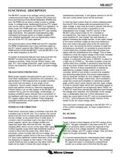
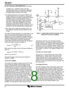
ErrorAmplifier Compensation
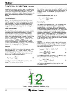
Oscillator (RAMP 1)
The oscillator frequency is determined by the values of R
The PWM loading of the PFC can be modeled as a
negative resistor; an increase in input voltage to the PWM
causes a decrease in the input current. This response
dictates the proper compensation of the two
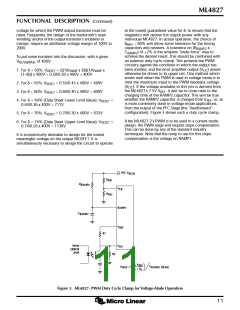
transconductance error amplifiers. Figure 2 shows the
types of compensation networks most commonly used for
the voltage and current error amplifiers, along with their
respective return points. The current loop compensation is
T
and C , which determine the ramp and off-time of the
T
oscillator output clock:
1
fOSC
=
(2)
(3)
tRAMP + tDEADTIME
The deadtime of the oscillator is derived from the
following equation:
returned to V
to produce a soft-start characteristic on
REF
the PFC: as the reference voltage comes up from zero
volts, it creates a differentiated voltage on IEAO which
prevents the PFC from immediately demanding a full duty
cycle on its boost converter.
F
H
I
K
V
-1.25
- 3.75
REF
= C ´R ´InGV
T
J
tRAMP
T
REF
at V
= 7.5V:
REF
There are two major concerns when compensating the
voltage loop error amplifier; stability and transient
response. Optimizing interaction between transient
response and stability requires that the error amplifier’s
open-loop crossover frequency should be 1/2 that of the
line frequency, or 23Hz for a 47Hz line (lowest
anticipated international power frequency). The gain vs.
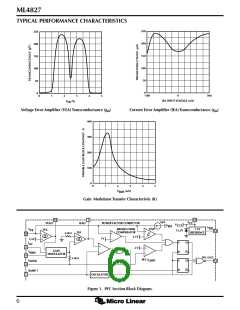
input voltage of the ML4827’s voltage error amplifier has
a specially shaped nonlinearity such that under steady-
state operating conditions the transconductance of the
error amplifier is at a local minimum. Rapid perturbations
in line or load conditions will cause the input to the
tRAMP = CT ´RT ´0.51
The deadtime of the oscillator may be determined using:
2.5V
tDEADTIME
=
´ CT = 490 ´ CT
(4)
5.1mA
The deadtime is so small (t
operating frequency can typically be approximated by:
>> t
) that the
RAMP
DEADTIME
1
fOSC
=
(5)
voltage error amplifier (V ) to deviate from its 2.5V
tRAMP
FB
(nominal) value. If this happens, the transconductance of
the voltage error amplifier will increase significantly, as
shown in the Typical Performance Characteristics. This
raises the gain-bandwidth product of the voltage loop,
resulting in a much more rapid voltage loop response to
such perturbations than would occur with a conventional
linear gain characteristic.
EXAMPLE:
For the application circuit shown in the data sheet, with
the oscillator running at:
1
fOSC = 100kHz =
tRAMP
-5
The current amplifier compensation is similar to that of
the voltage error amplifier with the exception of the
choice of crossover frequency. The crossover frequency of
the current amplifier should be at least 10 times that of
the voltage amplifier, to prevent interaction with the
voltage loop. It should also be limited to less than 1/6th
that of the switching frequency, e.g. 16.7kHz for a
100kHz switching frequency.
tRAMP = CT ´ RT ´ 0.51= 1´ 10
-4
Solving for R x C yields 2 x 10 . Selecting standard
components values, C = 470pF, and R = 41.2kΩ.
T
T
T
T
The deadtime of the oscillator adds to the Maximum
PWM Duty Cycle (it is an input to the Duty Cycle
Limiter). With zero oscillator deadtime, the Maximum
PWM Duty Cycle is typically 45% for the ML4827-1. In
many applications of the ML4827-1, care should be taken
that C not be made so large as to extend the Maximum
Duty Cycle beyond 50%. This can be accomplished by
There is a modest degree of gain contouring applied to the
transfer characteristic of the current error amplifier, to
increase its speed of response to current-loop
T
perturbations. However, the boost inductor will usually be
the dominant factor in overall current loop response.
Therefore, this contouring is significantly less marked than
that of the voltage error amplifier.
using a stable 470pF capacitor for C .
T
For more information on compensating the current and
voltage control loops, see Application Notes 33 and 34.
Application Note 16 also contains valuable information
for the design of this class of PFC.
9

 MICRO-LINEAR [ MICRO LINEAR CORPORATION ]