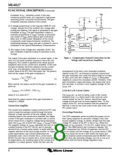
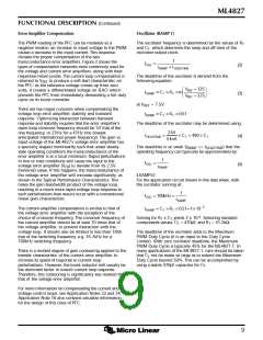
ML4827
FUNCTIONAL DESCRIPTION (Continued)
It is important that the time constant of the PWM soft-start
allow the PFC time to generate sufficient output power for
the PWM section. The PWM start-up delay should be at
least 5ms.
Using the recommended values of δ
= 60% and δ
MAX
MIN
= 64% for a high-δ application, a MOSFET switch with a
Drain-Source breakdown voltage of 900V, or in some
cases as low as 800V, can reliably be used. Such parts are
readily and inexpensively available from a number of
vendors.
Solving for the minimum value of C :
SS
50µA
V
OK Comparator
IN
CSS = 5ms ×
220nF
1.25V
The V OK comparator monitors the DC output of the
PFC and inhibits the PWM if this voltage on V is less
IN
Generating V
CC
FB
than its nominal 2.5V. Once this voltage reaches 2.5V,
which corresponds to the PFC output capacitor being
charged to its rated boost voltage, the soft-start begins.
The ML4827 is a current-fed part. It has an internal shunt
voltage regulator, which is designed to regulate the
voltage internal to the part at 13.5V. This allows a low
power dissipation while at the same time delivering 10V
of gate drive at the PWM OUT and PFC OUT outputs. It is
important to limit the current through the part to avoid
overheating or destroying it. This can be easily done with
PWM Control (RAMP 2)
When the PWM section is used in current mode, RAMP 2
is generally used as the sampling point for a voltage
representing the current in the primary of the PWM’s
output transformer, derived either by a current sensing
resistor or a current transformer. In voltage mode, it is the
input for a ramp voltage generated by a second set of
a single resistor in series with the V pin, returned to a
CC
bias supply of typically 18V to 20V. The resistor’s value
must be chosen to meet the operating current requirement
of the ML4827 itself (19mA max) plus the current required
by the two gate driver outputs.
timing components (R
, C
), which will have a
RAMP2
RAMP2
minimum value of zero volts and should have a peak
value of approximately 5V. In voltage mode operation,
feedforward from the PFC output buss is an excellent way
to derive the timing ramp for the PWM stage.
EXAMPLE:
With a V
of 20V, a V limit of 14.6V (max) and the
CC
BIAS
ML4827 driving a total gate charge of 110nC at 100kHz
(e.g., 1 IRF840 MOSFET and 2 IRF830 MOSFETs), the
gate driver current required is:
Soft Start
IGATEDRIVE = 100kHz ´ 100nC = 11mA
(7)
(8)
Start-up of the PWM is controlled by the selection of the
external capacitor at SS. A current source of 50µA
supplies the charging current for the capacitor, and start-
up of the PWM begins at 1.25V. Start-up delay can be
programmed by the following equation:
20V - 14.6V
RBIAS
=
= 180Ω
19mA + 11mA
To check the maximum dissipation in the ML4827, find
the current at the minimum V (12.4V):
50µA
´
CC
CSS = tDELAY
(6)
1.25V
20V - 12.4V
ICC
=
= 42.2mA
(9)
where C is the required soft start capacitance, and
SS
180Ω
t
is the desired start-up delay.
DELAY
The maximum allowable I is 55mA, so this is an
CC
acceptable design.
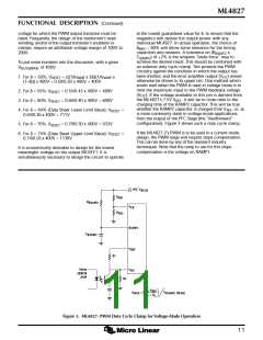
V
BIAS
R
BIAS
V
CC
ML4827
GND
10nF
CERAMIC
1µF
CERAMIC
Figure 4. External Component Connections to V
CC
12

 MICRO-LINEAR [ MICRO LINEAR CORPORATION ]