Trip le -Ou t p u t P o w e r-S u p p ly
Co n t ro lle r fo r No t e b o o k Co m p u t e rs
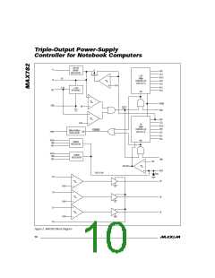
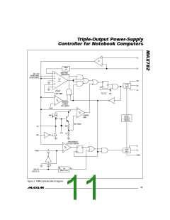
Hig h -S id e S u p p ly (VDD)
Table 2. VPP Program Codes
The 15V VDD supply is obtained from the rectified and
filtered secondary of transformer L2. VDD is enabled
whenever the +5V supply is on (ON5 = high). The pri-
mary and secondary of L2 are connected so that, dur-
ing the flyback portion of each cycle (when MOSFET
N2 is off and N4 is on), energy stored in the core is
transferred into the +5V load through the primary and
into VDD through the secondary, as determined by the
turns ratio. The secondary voltage is added to the +5V
DA0
DA1
VPPA
0
0
1
1
0
1
0
1
0V
5V
12V
Hi-Z
MAX782
DB0
DB1
VPPB
0
0
1
1
0
1
0
1
0V
5V
12V
Hi-Z
to ma ke VDD.
Se e the Typ ic a l Op e ra ting
Characteristics for the VDD supply’s load capability.
Unlike other coupled-inductor flyback converters, the
VDD voltage is regulated regardless of the loading on
the +5V output. (Most coupled-inductor converters can
only support the auxiliary output when the main output
is loaded.) When the +5V supply is lightly loaded, the
circuit achieves good control of VDD by pulsing the
MOSFET normally used as the synchronous rectifier.
This draws energy from the +5V supply’s output capac-
itor and uses the transformer in a forward-converter
mode (i.e., the +15V output takes energy out of the
s e c ond a ry whe n c urre nt is flowing in the p rima ry).
Note that these forward-converter pulses are inter-
spersed with normal synchronous-rectifier pulses, and
they only occur at light loads on the +5V rail.
ply (VDD), and each can furnish up to 60mA. Bypass
VPPA and VPPB to GND with at least 1µF, with the
bypass capacitors less than 20mm from the VPP pins.
The outputs are programmed with DA0, DA1, DB0 and
DB1, as shown in Table 2.
These codes are Intel 82365 (PCMCIA digital controller)
compatible. For other interfaces, one of the inputs can
be permanently wired high or low and the other toggled
to turn the supply on and off. The truth table shows that
either a “0” or “1” can be used to turn each supply on.
The high-impedance state is to accomodate external
programming voltages. The two VPP outputs can be
safely connected in parallel for increased load capability
if the control inputs are also tied together (i.e., DA0 to
DB0, DA1 to DB1). If VPAA and VPPB are connected in
parallel, some devices may exhibit several milliamps of
increased quiescent supply current when enabled, due
to slightly mismatched output voltage set points.
The transformer secondary’s rectified and filtered out-
put is only roughly regulated, and may be between 13V
and 19V. It is brought back into VDD, which is also the
feedback input, and used as the source for the PCMCIA
VPP regulators (see Generating Additional VPP Outputs
Using External Linear Regulators). It can also be used
as the VH power supply for the comparators or any
external MOSFET drivers.
Co m p a ra t o rs
Three noninverting comparators can be used as preci-
sion voltage comparators or high-side drivers. The
supply for these comparators (VH) is brought out and
may be connected to any voltage between +3V and
+19V. The noninverting inputs (D1-D3) are high imped-
ance, and the inverting input is internally connected to
a 1.650V reference. Each output (Q1-Q3) sources
20µA from VH when its input is above 1.650V, and
sinks 500µA to GND when its input is below 1.650V.
The Q1-Q3 outputs can be fixed together in wired-OR
configuration since the pull-up current is only 20µA.
When the input voltage is above 20V, or when the +5V
supply is heavily loaded and VDD is lightly loaded, L2’s
interwinding capacitance and leakage inductance can
produce voltages above that calculated from the turns
ratio. A 3mA shunt regulator limits VDD to 19V.
Clock-frequency noise on the VDD rail of up to 3Vp-p is
a facet of normal operation, and can be reduced by
adding more output capacitance.
P CMCIA-Co m p a t ib le
P ro g ra m m a b le VP P S u p p lie s
Two independent regulators are provided to furnish
PCMCIA VPP supplies. The VPPA and VPPB outputs
can be programmed to deliver 0V, 5V, 12V, or to be high
impedance. The 0V output mode has a 250Ω pull-down
to discharge external filter capacitors and ensure that
flash EPROMs cannot be accidentally programmed.
These linear regulators operate from the high-side sup-
Connecting VH to a logic supply (5V or 3V) allows the
comparators to be used as low-battery detectors. For dri-
ving N-channel power MOSFETs to turn external loads on
and off, VH should be 6V to 12V higher than the load volt-
age. This enables the MOSFETs to be fully turned on and
results in low r . VDD is a convenient source for VH.
DS(ON)
14 ______________________________________________________________________________________

 MAXIM [ MAXIM INTEGRATED PRODUCTS ]