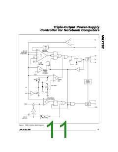
Trip le -Ou t p u t P o w e r-S u p p ly
Co n t ro lle r fo r No t e b o o k Co m p u t e rs
MAX782
The comparators are always active when V+ is above
as no-load (standby) operation when a battery charger
+4V, even when VH is 0V. Thus, Q1-Q3 will sink current
to GND even when VH is 0V, but they will only source
current from VH when VH is above approximately 1.5V.
is connected but no battery is installed.
not exceed 30V.
V
can-
IN(MAX)
V
, the minimum input (battery) voltage. This
IN(MIN)
If Q1, Q2, or Q3 is externally pulled above VH, an inter-
nal diode conducts, pulling VH a diode drop below the
output and powering anything connected to VH. This
voltage will also power the other comparator outputs.
value should be taken at the full-load operating cur-
rent under the lowest battery conditions. If V
IN(MIN)
is b e low a b out 6.5V, the p owe r a va ila b le from the
VDD supply will be reduced. In addition, the filter
capacitance required to maintain good AC load reg-
ulation increases, and the current limit for the +5V
supply has to be increased for the same load level.
In t e rn a l VL a n d REF S u p p lie s
An internal linear regulator produces the 5V used by the
internal control circuits. This regulator’s output is avail-
able on pin VL and can source 5mA for external loads.
Bypass VL to GND with 4.7µF. To save power, when
the +5V switch-mode supply is above 4.5V, the internal
linear regulator is turned off and the high-efficiency +5V
switch-mode supply output is connected to VL.
+3 .3 V In d u c t o r (L1 )
Three inductor parameters are required: the inductance
value (L), the peak inductor current (I ), and the
LPEAK
coil resistance (R ). The inductance is:
L
V
OUT
x (V
- V
)
IN(MAX)
OUT
The internal 3.3V bandgap reference (REF) is powered
by the internal 5V VL supply, and is always on. It can
furnish up to 5mA. Bypass REF to GND with 0.22µF,
plus 1µF/mA of load current.
L = ————————————-
x f x I x LIR
V
IN(MAX)
OUT
where:
V
OUT
= output voltage, 3.3V;
V
= maximum input voltage (V);
IN(MAX)
Both the VL and REF outputs remain active, even when
the switching regulators are turned off, to supply mem-
ory keep-alive power.
f = switching frequency, normally 300kHz;
= maximum +3.3V DC load current (A);
LIR = ratio of inductor peak-to-peak AC
I
OUT
These linear-regulator ouputs can be directly connected
to the corresponding step-down regulator outputs (i.e.,
REF to +3.3V, VL to +5V) to keep the main supplies alive
in standby mode. However, to ensure start-up, standby
load currents must not exceed 5mA on each supply.
current to average DC load current, typically 0.3.
A higher value of LIR allows smaller inductance, but
results in higher losses and higher ripple.
The highest peak inductor current (I ) equals the
LPEAK
DC load current (I ) plus half the peak-to-peak AC
OUT
inductor current (I ). The peak-to-peak AC inductor
current is typically chosen as 30% of the maximum DC
load current, so the peak inductor current is 1.15 times
Fault Protection
The +3.3V and +5V PWM supplies, the high-side sup-
ply, and the comparators are disabled when either of
two faults is present: VL < +4.0V or REF < +2.8V (85%
of its nominal value).
LPP
I
.
OUT
The peak inductor current at full load is given by:
x (V - V
V
OUT
)
OUT
__________________De s ig n P ro c e d u re
IN(MAX)
I
= I
OUT
+ —————————————.
LPEAK
Figure 1’s schematic and Table 2’s component list
show values suitable for a 3A, +5V supply and a 3A,
+3.3V supply. This circuit operates with input voltages
from 6.5V to 30V, and maintains high efficiency with
output currents between 5mA and 3A (see the Typical
Operating Characteristics). This circuit’s components
may be changed if the design guidelines described in
this section are used – but before beginning the design,
the following information should be firmly established:
2 x f x L x V
IN(MAX)
The c oil re s is ta nc e s hould b e a s low a s p os s ib le ,
preferably in the low milliohms. The coil is effectively in
series with the load at all times, so the wire losses alone
are approximately:
2
Power loss = I
x R
L
OUT
In general, select a standard inductor that meets the L,
, and R requirements (see Tables 3 and 4). If a
I
LPEAK
L
V , the maximum input (battery) voltage. This
IN(MAX)
standard inductor is unavailable, choose a core with an
value should include the worst-case conditions under
which the power supply is expected to function, such
2
2
LI parameter greater than L x I
, and use the
LPEAK
largest wire that will fit the core.
______________________________________________________________________________________ 15

 MAXIM [ MAXIM INTEGRATED PRODUCTS ]