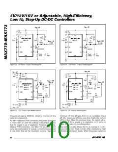
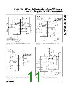
5 V/1 2 V/1 5 V o r Ad ju s t a b le , High-Effic ie nc y,
Low I , Ste p-Up DC-DC Controlle rs
Q
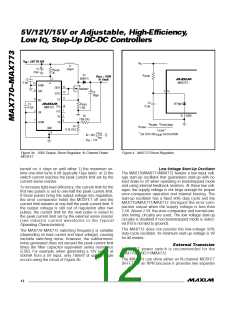
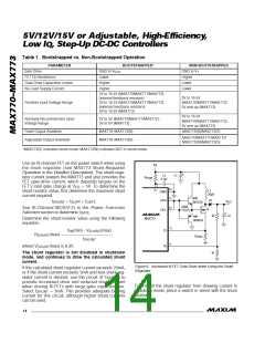
Table 1. Bootstrapped vs. Non-Bootstrapped Operation
PARAMETER
BOOTSTRAPPED*
NON-BOOTSTRAPPED
GND to V+
Gate Drive
GND to V
OUT
FET On Resistance
Lower
Higher
Higher
Higher
Lower
Lower
Gate-Drive Capacitive Losses
No-Load Supply Current
2V to 16.5V (MAX770/MAX771/MAX772),
(internal feedback resistors)
3V to 16.5V
Possible Input Voltage Range
3V to 16.5V (MAX770/MAX771/MAX772),
(external feedback resistors)
(MAX770/MAX771/MAX772),
3V and up (MAX773)
3V to 16.5V (MAX773)
5V to 16.5V
(MAX770/MAX771/MAX772),
5V and up (MAX773)
Normally Recommended Input
Voltage Range
2V to 5V (MAX770/MAX771/MAX772),
3V to 5V (MAX773)
Fixed Output Available
MAX770–MAX773(N)
MAX770–MAX773(N)
MAX773(N)/MAX773(S)
0–MAX73
MAX770/MAX771/MAX772/
MAX773(N)/MAX773(S)
Adjustable Output Available
*MAX773(S) indicates shunt mode; MAX773(N) indicates NOT in shunt mode.
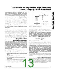
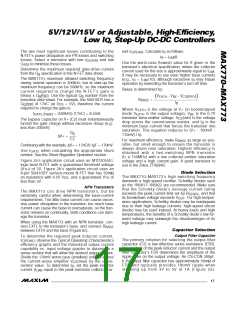
Use an N-channel FET as the power switch when using
the s hunt re g ula tor (s e e MAX773 Shunt-Re g ula tor
Operation in the Detailed Description). The shunt-regu-
lator current powers the MAX773 and also provides the
FET gate-drive current, which depends largely on the
V
IN
C2
0.1µF
C1
R
SHUNT
3
FET’s total gate charge at V = 5V. To determine the
GS
10
13
V+
L1
20µH
shunt-resistor value, first determine the maximum shunt
current required.
SGND
EXTH
NPN
2N2222A
D1
V
OUT
I
= I
+ I
SHUNT
SUPP GATE
100Ω
Se e N-Cha nne l MOSFETs in the Powe r-Tra ns is tor
Selection section to determine I
12
N
EXTL
.
GATE
R2
C4
PNP
2N2907A
MAX773
Determine the shunt-resistor value using the following
equation:
11
6
CS
FB
V (min) - V
(max)
IN
SHUNT
R
(max) = ————————————
SHUNT
R
SENSE
I
SHUNT
where V
(max) is 6.3V.
SHUNT
The shunt regulator is not disabled in shutdown
mode, and continues to draw the calculated shunt
current.
R1
Figure 6. Increased N-FET Gate Drive when Using the Shunt
Regulator
If the calculated shunt regulator current exceeds 20mA,
or if the shunt current exceeds 5mA and less shunt reg-
ulator current is desired, use the circuit of Figure 6 to
provide increased drive and reduced shunt current
when driving N-FETs with large gate capacitances.
To prevent the shunt regulator from drawing current in
shutdown mode, place a switch in series with the shunt
resistor.
Select I
= 3mA. This provides adequate biasing
SHUNT
current for this circuit, although higher shunt currents
can be used.
______________________________________________________________________________________
14

 MAXIM [ MAXIM INTEGRATED PRODUCTS ]