5 V/1 2 V/1 5 V o r Ad ju s t a b le , High-Effic ie nc y,
Low I , Ste p-Up DC-DC Controlle rs
Q
0–MAX73
The two most sig nific a nt losse s c ontributing to the
N-FET’s power dissipation are I R losses and switching
rent I
. Calculate I as follows:
C(PEAK) B
2
I = I /ß
B
LIM
losses. Select a transistor with low r
and low
DS(ON)
Use the worst-case (lowest) value for ß given in the
transistor’s electrical specification, where the collector
current used for the test is approximately equal to I
It may be necessary to use even higher base currents
(e.g., I = I /10), although excessive I may impair
operation by extending the transistor’s turn-off time.
C
to minimize these losses.
RSS
Determine the maximum required gate-drive current
.
LIM
from the Q specification in the N-FET data sheet.
g
The MAX773’s maximum allowed switching frequency
during normal operation is 300kHz; but at start-up the
maximum frequency can be 500kHz, so the maximum
c urre nt re q uire d to c ha rg e the N-FET’s g a te is
B
LIM
B
R
is determined by:
BASE
f(max) x Q (typ). Use the typical Q number from the
g
g
V
- V - V
BE CS
(
(min ))
EXTH
transistor data sheet. For example, the Si9410DY has a
Q (typ) of 17nC (at V = 5V), therefore the current
R
BASE
= ————————————–
I
B
g
GS
required to charge the gate is:
Where V
mode V
is the voltage at V+ (in bootstrapped
EXTH
is the output voltage), V is the 0.7V
EXTH BE
I
= (500kHz) (17nC) = 8.5mA.
GATE
(max)
transistor base-emitter voltage, V (min) is the voltage
drop across the current-sense resistor, and I is the
minimum base current that forces the transistor into
saturation. This equation reduces to (V+ - 700mV -
170mV) / I .
CS
The bypass capacitor on V+ (C2) must instantaneously
furnish the gate charge without excessive droop (e.g.,
less than 200mV):
B
Q
g
B
∆V+ = ——
C2
For maximum efficiency, make R
as large as pos-
BASE
s ib le , b ut s ma ll e noug h to e ns ure the tra ns is tor is
always driven near saturation. Highest efficiency is
ob ta ine d with a fa s t-s witc hing NPN tra ns is tor
Continuing with the example, ∆V+ = 17nC/0.1µF = 170mV.
Us e I
whe n c a lc ula ting the a p p rop ria te s hunt
GATE
resistor. See the Shunt Regulator Operation section.
(f ≥ 150MHz) with a low collector-emitter saturation
T
Figure 2a’s application circuit uses an MTD3055EL
logic-level N-FET with a guaranteed threshold voltage
(V ) of 2V. Figure 2b’s application circuit uses an
TH
voltage and a high current gain. A good transistor to
use is the Zetex ZTX694B.
Dio d e S e le c t io n
The MAX770–MAX773’s hig h s witc hing fre q ue nc y
demands a high-speed rectifier. Schottky diodes such
as the 1N5817–1N5822 are recommended. Make sure
tha t the Sc hottky d iod e ’s a ve ra g e c urre nt ra ting
8-pin Si9410DY surface-mount N-FET that has 50mΩ
on resistance with 4.5V V , and a guaranteed V of
GS
TH
less than 3V.
NPN Transistors
The MAX773 c a n d rive NPN tra ns is tors , b ut b e
extremely careful when determining the base-current
requirements. Too little base current can cause exces-
sive power dissipation in the transistor; too much base
current can cause the base to oversaturate, so the tran-
sistor remains on continually. Both conditions can dam-
age the transistor.
exceeds the peak current limit set by R , and that
SENSE
its breakdown voltage exceeds V . For high-temper-
OUT
ature applications, Schottky diodes may be inadequate
due to their high leakage currents; high-speed silicon
diodes may be used instead. At heavy loads and high
temperatures, the benefits of a Schottky diode’s low for-
ward voltage may outweigh the disadvantages of its
high leakage current.
When using the MAX773 with an NPN transistor, con-
nect EXTL to the transistor’s base, and connect R
between EXTH and the base (Figure 8c).
BASE
Ca p a c it o r S e le c t io n
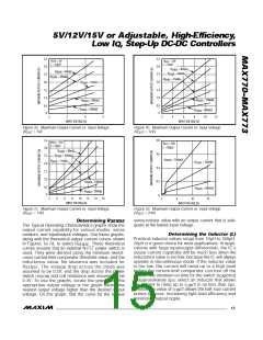
Output Filter Capacitor
The p rima ry c rite rion for s e le c ting the outp ut filte r
capacitor (C2) is low effective series resistance (ESR).
The product of the peak inductor current and the output
filter capacitor’s ESR determines the amplitude of the
ripple seen on the output voltage. An OS-CON 300µF,
6.3V output filter capacitor has approximately 50mΩ of
ESR a nd typ ic a lly p rovid e s 180mV rip p le whe n
s te p p ing up from 3V to 5V a t 1A (Fig ure 2a ).
To d e te rmine the re q uire d p e a k ind uc tor c urre nt,
), observe the Typical Operating Characteristics
efficiency graphs and the theoretical output current
c a p a b ility vs . inp ut volta g e g ra p hs to d e te rmine a
sense resistor that will allow the desired output current.
Divide the 170mV worst-case (smallest) voltage across
I
C(PEAK
the current-sense amplifier V (max) by the sense-
CS
resistor value. To determine I , set the peak inductor
B
current (I
equal to the peak transistor collector cur-
LIM)
______________________________________________________________________________________
17

 MAXIM [ MAXIM INTEGRATED PRODUCTS ]