5 V/1 2 V/1 5 V o r Ad ju s t a b le , High-Effic ie nc y,
Low I , Ste p-Up DC-DC Controlle rs
Q
0–MAX73
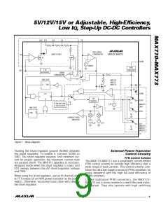
drive outputs (EXTH and EXTL) that operate 180° out of
phase (Figures 3a and 3b). In Figure 3b, the resistor in
series with EXTH limits the base current, and EXTL (which
is connected directly to the base) turns the transistor off.
R2
V
OUT
FB
R1
S h u t d o w n Mo d e
When SHDN is high, the MAX770–MAX773 enter shut-
down mode. In this mode, the internal biasing circuit-
MAX770
MAX771
MAX772
MAX773
ry is turne d off (inc lud ing the re fe re nc e ) a nd V
OUT
falls to a diode drop below V (due to the DC path
IN
R1 = 10k TO 500k
from the input to the output). In shutdown mode, the
s up p ly c urre nt d rop s to le s s tha n 5µA. SHDN is a
TTL/CMOS logic-level input. Connect SHDN to GND for
normal operation.
V
GND
OUT
R2 = R1
-1
(
)
V
REF
V
REF
= 1.5V
The MAX773’s shunt regulator is not disabled in shut-
down mode.
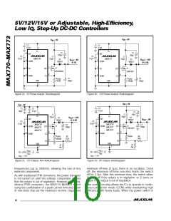
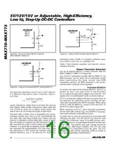
Figure 5. Adjustable Output Circuit
Lo w -Ba t t e ry De t e c t o r
The MAX773 provides a low-battery comparator that
compares the voltage on LBI to the reference voltage.
See Table 1 for a summary of operating characteristics
and requirements for the ICs in bootstrapped and non-
bootstrapped modes.
When the LBI voltage is below V
LBO (an open-
,
REF
The MAX770–MAX773’s output voltage can be adjust-
ed from very high voltages down to 3V, using external
resistors R1 and R2 configured as shown in Figure 5.
For adjustable-output operation, select feedback resis-
tor R1 in the range of 10kΩ to 500kΩ. R2 is given by:
drain output) goes low. The low-battery comparator’s
20mV of hysteresis adds noise immunity, preventing
repeated triggering of LBO. Use a resistor-divider network
between V+, LBI, and GND to set the desired trip voltage
V
TRIP
. LBO is high impedance in shutdown mode.
V
OUT
R2 = (R1) ––––– -1
(
)
__________________De s ig n P ro c e d u re
V
REF
S e t t in g t h e Ou t p u t Vo lt a g e
To set the output voltage, first determine the mode of
operation, either bootstrapped or non-bootstrapped.
Boots tra p p e d mod e p rovid e s more outp ut c urre nt
capability, while non-bootstrapped mode reduces the
supply current (see Typical Operating Characteristics).
If a decaying voltage source (such as a battery) is
used, see the additional notes in the Low Input Voltage
Operation section.
where V
equals 1.5V.
REF
For p re s e t-outp ut op e ra tion, tie FB to GND (this
forc e s b oots tra p p e d -mod e op e ra tion for the
MAX770/MAX771/MAX772).
Configure the MAX773 for a preset voltage of 5V, 12V, or
15V b y c onne c ting the output to the c orre sp onding
sense input pin (i.e., V5, V12, or V15). FB must be tied to
ground for preset-output operation. Leave all unused
sense input pins unconnected. Failure to do so will cause
an incorrect output voltage. The MAX773 can provide
a preset output voltage in both bootstrapped and non-
bootstrapped modes.
Use the MAX770/MAX771/MAX772 unless one or more
of the following conditions applies. If one or more of the
following is true, use the MAX773:
1) An NPN power transistor will be used as the power
switch
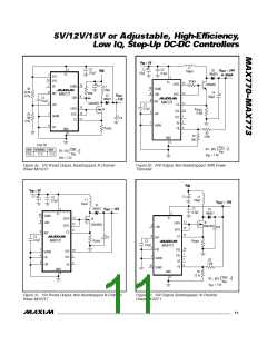
Figures 2 and 3 show various circuit configurations for
b oots tra p p e d /non-b oots tra p p e d , p re s e t/a d jus ta b le
operation.
2) The LBI/LBO function is required
S h u n t -Re g u la t o r Op e ra t io n
When using the shunt regulator, connect SGND to ground
and place a 0.1µF capacitor between V+ and SGND, as
close to the IC as possible. Increase C2 to 1.0µF to
improve shunt regulators performance with heavy loads.
3) The shunt regulator must accommodate a high
input voltage
4) Preset-output non-bootstrapped operation is
desired—for example, to reduce the no-load
supply current in a 5V to 12V application.
Select R
such that 1mA ≤ I
≤ 20mA.
SHUNT
SHUNT
______________________________________________________________________________________
13

 MAXIM [ MAXIM INTEGRATED PRODUCTS ]