5 V/1 2 V/1 5 V o r Ad ju s t a b le , High-Effic ie nc y,
Low I , Ste p-Up DC-DC Controlle rs
Q
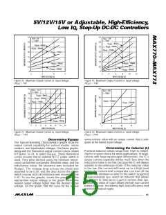
Smaller capacitors are acceptable for light loads or in
applications that can tolerate higher output ripple.
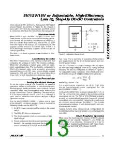
V
IN
Since the output filter capacitor’s ESR affects efficien-
cy, use low-ESR capacitors for best performance. The
smallest low-ESR surface-mount tantalum capacitors
V+
R4
R5
100k
currently available are the Sprague 595D series. Sanyo
OS-CON organic semiconductor through-hole capaci-
tors and the Nichicon PL series also exhibit low ESR.
MAX773
LBI
LBO
LOW-BATTERY
OUTPUT
R3
See Table 2.
Input Bypass Capacitors
The input bypass capacitor (C1) reduces peak currents
drawn from the voltage source and also reduces noise
at the voltage source caused by the switching action of
the MAX770–MAX773. The input voltage source imped-
ance determines the size of the capacitor required at
the V+ input. As with the output filter capacitor, a low-
ESR capacitor is recommended. For output currents up
to 1A, 150µF (C1) is a d e q ua te , a lthoug h s ma lle r
bypass capacitors may also be acceptable.
GND
V
TRIP
R4 = R3
-1
)
(
V
REF
V
REF
= 1.5V
Figure 9. Input Voltage Monitor Circuit
0–MAX73
__________Ap p lic a t io n s In fo rm a t io n
MAX7 7 3 Op e ra t io n w it h Hig h
In p u t /Ou t p u t Vo lt a g e s
Bypass the IC with a 0.1µF ceramic capacitor (C2)
placed close to the V+ and GND pins.
The MAX773’s shunt regulator input allows high volt-
ages to be converted to very high voltages. Since the
MAX773 runs off the 6V shunt (bootstrapped operation
is not allowed), the IC will not see the high input volt-
age. Use an external logic-level N-FET as the power
Reference Capacitor
Byp a s s REF with a 0.1µF c a p a c itor (C3). REF c a n
source up to 100µA of current.
S e t t in g t h e Lo w -Ba t t e ry-De t e c t o r Vo lt a g e
To set the low-battery detector’s falling trip voltage
switch, since only 6V of V are available. Also, make
GS
sure all external components are rated for very high
output voltage. Figure 3e shows a circuit that converts
28V to 100V.
(V
TRIP
(falling)), select R3 between 10kΩ and 500kΩ
(Figure 9), and calculate R4 as follows:
VTRIP - VREF
Lo w In p u t Vo lt a g e Op e ra t io n
Whe n us ing a p owe r s up p ly tha t d e c a ys with time
(such as a battery), the N-FET transistor will operate in
its linear region when the voltage at EXT approaches
the threshold voltage of the FET, dissipating excessive
power. Prolonged operation in this mode may damage
the FET. This effect is much more significant in non-
bootstrapped mode than in bootstrapped mode, since
bootstrapped mode typically provides much higher
R4 = (R3) ———————
(
)
V
REF
where V
= 1.5V.
REF
The rising trip voltage is higher because of the com-
parator’s approximately 20mV of hysteresis, and is
determined by:
R4
V
(rising) = (V
+ 20mV) (1 + ——)
TRIP
REF
R3
V
voltages. To avoid this condition, make sure V
GS
EXT
is above the V of the FET, or use a voltage detector
TH
Connect a high value resistor (larger than R3 + R4)
between LBI and LBO if additional hysteresis is required.
(such as the MAX8211) to put the IC in shutdown mode
once the input supply voltage falls below a predeter-
mined minimum value. Excessive loads with low input
voltages can also cause this condition.
Connect a pull-up resistor (e.g., 100kΩ) between LBO
and V+. Tie LBI to GND and leave LBO floating if the
low-battery detector is not used.
______________________________________________________________________________________
18

 MAXIM [ MAXIM INTEGRATED PRODUCTS ]