2x4-Channel, Simultaneous-Sampling
12-Bit ADCs
t
CW
CONVST
INT
t
t
ACQ
CONV
t
ID
t
CWH
t
CWS
CS
RD
t
CRS
t
CRH
t
RD
t
t
WR
RD
WR
t
DA
t
DH
DATA
CH1
CH2
CH3
CH4
DATA IN
t
AS
t
AH
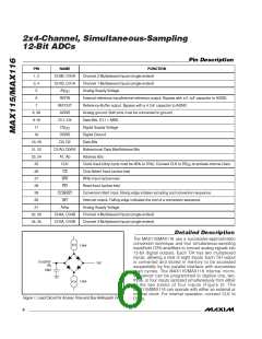
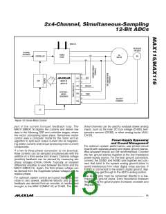
Figure 4. Timing Diagram
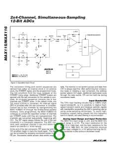
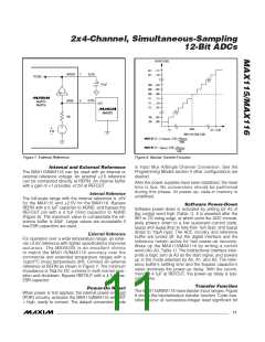
acquisition time between conversions. The analog input
appears as a 10k resistor in parallel with a 16pF
capacitor for the MAX115 and as a 1M resistor in par-
allel with a 16pF capacitor for the MAX116.
CS
WR
Between conversions, the buffer input is connected to
channel 1 of the selected track/hold bank. When a
channel is not selected, switches S1, S2, and S3 are
placed in hold mode to improve channel-to-channel
isolation.
A0
(LSB)
A1
A2
A3
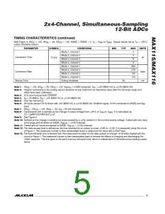
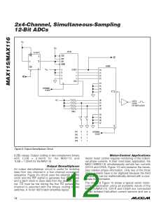
Digital Interface
Input data (A0–A3) and output data (D0–D11) are multi-
plexed on a three-state bidirectional interface. This par-
allel I/O can easily be interfaced with a microprocessor
(µP) or DSP. CS, WR, and RD control the write and read
operations. CS is the standard chip-select signal, which
enables the controller to address the MAX115/MAX116
as an I/O port. When CS is high, it disables the WR and
RD inputs and forces the interface into a high-Z state.
Figure 4 details the interface timing.
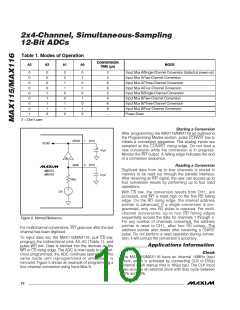
Figure 5. Programming a Four-Channel Conversion, Input Mux A
Track/Holds
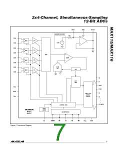
The MAX115/MAX116 feature four simultaneous T/Hs.
Each T/H has two multiplexed inputs. A T-switch input
configuration provides excellent hold-mode isolation.
Allow 600ns acquisition time for 12-bit accuracy.
Programming Modes
The MAX115/MAX116 have eight conversion modes
plus power-down, which are programmed through a
bidirectional parallel interface. At power-up, the devices
default to the Input Mux A/Single-Channel Conversion
mode. The user can select between two banks (mux
inputs A or mux inputs B) of four simultaneous-sampled
input channels, as illustrated in Figure 2. An internal
microsequencer can be programmed to convert one to
four channels of the selected bank per sample. For a
single-channel conversion, CH1 is digitized, and then
INT goes low to indicate completion of the conversion.
The T/H aperture delay is typically 10ns. The 500ps
aperture-delay mismatch between the T/Hs allows the
relative phase information of up to four different inputs
to be preserved. Figure 3 shows the equivalent input
circuit, illustrating the ADC’s sampling architecture.
Only one of four T/H stages with its two multiplexed
inputs (CH_A and CH_B) is shown. All switches are in
track configuration for channel A. An internal buffer
charges the hold capacitor to minimize the required
_______________________________________________________________________________________
9

 MAXIM [ MAXIM INTEGRATED PRODUCTS ]