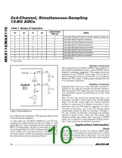
2x4-Channel, Simultaneous-Sampling
12-Bit ADCs
V
CC
V
CC
HC161
1/2 HC74
Q
PRE
D
CLR
ENP
ENT
RD
P = Q
G
Q
LOAD
HC688
CLR
V
(LSB) 0
1
CC
A
B
C
P0
P1
P2
P3
2
3
RCO
INT
D
P4
P5
P6
P7
EXTERNAL
CLOCK
V
CC
Q0
Q1
Q2
Q3
LATCH
CLOCK
(TO 16373 LATCH)
10k
Q4
Q5
Q6
Q7
CH1
CH2
CH3
CH4
0
1
0
1
0
0
1
1
EXTERNAL
CLOCK
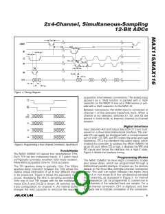
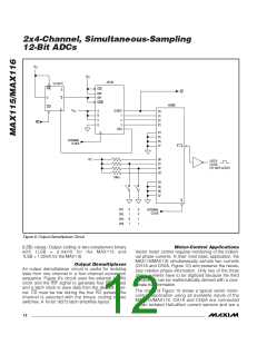
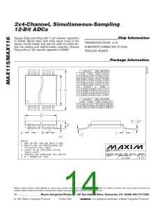
Figure 9. Output Demultiplexer Circuit
(LSB) values. Output coding is two-complement binary
with 1LSB 2.44mV for the MAX115 and
1LSB = 1.22mV for the MAX116.
Motor-Control Applications
=
Vector motor control requires monitoring of the individ-
ual phase currents. In their most basic application, the
MAX115/MAX116 simultaneously sample two currents
(CH1A and CH2A, Figure 10) and preserve the neces-
sary relative phase information. Only two of the three
phase currents have to be digitized because the third
component can be mathematically derived with a coor-
dinate transformation.
Output Demultiplexer
An output demultiplexer circuit is useful for isolating
data from one channel in a four-channel conversion
sequence. Figure 9’s circuit uses the external 16MHz
clock and the INT signal to generate four RD pulses
and a latch clock to save data from the desired chan-
nel. CS must be low during the four RD pulses. The
channel is selected with the binary coding of two
switches. A 16-bit 163ꢀ3 latch simplifies layout.
The circuit of Figure 10 shows a typical vector motor-
control application using all available inputs of the
MAX115/MAX116. CH1A and CH2A are connected
to two isolated Hall-effect current sensors and are a
12 ______________________________________________________________________________________

 MAXIM [ MAXIM INTEGRATED PRODUCTS ]