2x4-Channel, Simultaneous-Sampling
12-Bit ADCs
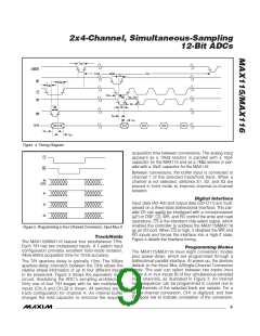
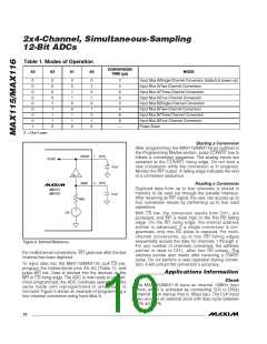
OUTPUT CODE
011 . . . 111
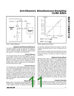
REFOUT
7
(2.5V)
011 . . . 110
TO DAC
4.7 F
000 . . . 010
000 . . . 001
000 . . . 000
A
V
= 1
111 . . . 111
111 . . . 110
111 . . . 101
(2.5V)
REFIN
10k
6
MAX115
MAX116
OUT
MAX6325
100 . . . 001
100 . . . 000
ZERO
- FS
+FS - 1LSB
2.5V
INPUT VOLTAGE (LSB)
MAX115: FS = 2 x V
, 1LSB = 4V
REFOUT
REFOUT
4096
MAX116: FS = V
, 1LSB = 2V
REFOUT
REFOUT
4096
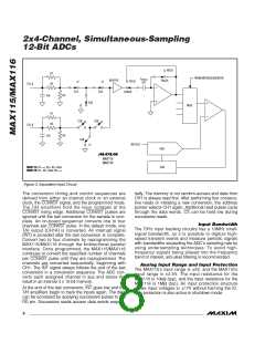
Figure 7. External Reference
Figure 8. Bipolar Transfer Function
is Input Mux A/Single Channel Conversion. See the
Programming Modes section if other configurations are
desired.
Internal and External Reference
The MAX115/MAX116 can be used with an internal or
external reference voltage. An external +2.5 reference
can be connected directly at REFIN. An internal buffer
with a gain of +1 provides +2.5V at REFOUT.
After the power supplies have been stabilized, the reset
time is 5µs. No conversions should be performed
during this phase. At power-up, data-in memory is
undefined.
Internal Reference
The full-scale range with the internal reference is 5V
for the MAX115 and 2.5V for the MAX116. Bypass
REFIN with a 0.1µF capacitor to AGND, and bypass the
REFOUT pin with a 4.ꢀµF (min) capacitor to AGND
(Figure 6). The maximum value to compensate the ref-
erence buffer is 22µF. Larger values are acceptable if
low-ESR capacitors are used.
Software Power-Down
Software power-down is activated by setting bit A3 of
the control word high (Table 1). It is asserted after the
WR or CS rising edge, at which point the ADC immedi-
ately powers down to a low quiescent-current state.
I
and I
drop to less than 1µA (typ), and I
AVSS DVDD
AVDD
drops to 13µA (typ). The ADC circuitry and reference
buffer are turned off, but the digital interface and the
reference remain active for fast power-up recovery.
Wake up the MAX115/MAX116 by writing a control
word (A0–A3, Table 1). The bidirectional interface inter-
prets a logic zero at A3 as the start signal, and powers
up in the mode selected by A0, A1, and A2. The refer-
ence buffer’s settling time and the bypass capacitor’s
value dominate the power-up delay. With the recom-
mended 4.ꢀµF at REFOUT, the power-up delay is typi-
cally 20ms.
External Reference
For operation over a wide temperature range, an exter-
nal +2.5V reference with tighter specifications improves
accuracy. The MAX6325 is an excellent choice
to match the MAX115/MAX116 accuracy over the
commercial and extended temperature ranges with a
1ppm/°C (max) temperature drift. Connect an external
reference at REFIN as shown in Figure ꢀ. The minimum
impedance is ꢀk for DC currents in both normal oper-
ation and shutdown. Bypass REFOUT with a 4.ꢀµF low-
ESR capacitor.
Transfer Function
The MAX115/MAX116 have bipolar input ranges. Figure
8 shows the bipolar/output transfer function. Code tran-
sitions occur at successive-integer least significant bit
Power-On Reset
When power is first applied, the internal power-on reset
(POR) circuitry activates the MAX115/MAX116 with INT
= high, ready to convert. The default conversion mode
______________________________________________________________________________________ 11

 MAXIM [ MAXIM INTEGRATED PRODUCTS ]