2x4-Channel, Simultaneous-Sampling
12-Bit ADCs
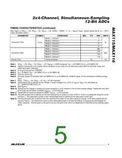
TIMING CHARACTERISTICS (continued)
(See Figure 4, AV
= +5V, AV = -5V, DV
= +5V, AGND = DGND = 0, T = T
A
to T
, Typical values are at T = +25°C,
MAX A
DD
SS
DD
MIN
unless otherwise noted.)
PARAMETER
SYMBOL
CONDITIONS
MIN
TYP
MAX
2
UNITS
Mode 1, Channel 1
Mode 2, Channel 2
Mode 3, Channel 3
Mode 4, Channel 4
Mode 1, Channel 1
Mode 2, Channel 2
Mode 3, Channel 3
Mode 4, Channel 4
Exiting shutdown
4
Conversion Time
t
µs
CONV
6
8
390
218
152
116
Conversion Rate
Startup Time
ksps
ms
20
Note 1: AV
= +5V, AV = -5V, DV
= +5V, V
= 2.500V (external), V
= 5V (MAX115) or 2.5V (MAX116).
DD
SS
DD
REFIN
IN
Note 2: Integral nonlinearity is the analog value’s deviation at any code from its theoretical value after the full-scale range and
offset have been calibrated.
Note 3: CLK synchronized with CONVST.
Note 4:
f
IN
= 10.06kHz, V
= 5V (MAX115) or 2.5V (MAX116).
IN
Note 5: First five harmonics.
Note 6: All inputs except CH1A driven with 5V (MAX115) or 2.5V (MAX116) 10.06kHz signal, CH1A connected to AGND and digi-
tized.
Note 7: AV
= DV
= +5V, AV = -5V, V = 0V (all channels).
DD SS IN
DD
Note 8: Temperature drift is defined as the change in output voltage from +25°C to T
TC = [ REFOUT/REFOUT] / T.
or T
. It is calculated as
MAX
MIN
Note 9: See Figure 2.
Note 10: Defined as the change in positive full scale caused by a 5ꢁ variation in the nominal supply voltage. Tested with one input
at full scale and all others at AGND. V = +2.5V (internal).
REFIN
Note 11: Tested with all inputs connected to AGND. V
= +2.5V (internal).
REFIN
Note 12: The data access time is defined as the time required for an output to cross +0.8V or +2.0V. It is measured using the circuit
of Figure 1. The measured number is then extrapolated back to determine the value with a 25pF load.
Note 13: The bus relinquish time is derived from the measured time taken for the data outputs to change +0.5V when loaded with the
circuit of Figure 1. The measured number is then extrapolated back to remove the effects of charging and discharging the
120pF capacitor. The time given is the part’s true bus relinquish time, which is independent of the external bus loading capac-
itance.
_______________________________________________________________________________________
5

 MAXIM [ MAXIM INTEGRATED PRODUCTS ]