8- and 4-Channel, 3 ꢀ ꢁREF
Multirange Inputs, Serial 14-Bit ADCs
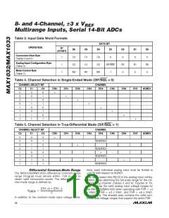
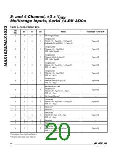
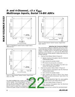
FSR
FSR
3FFF
3FFE
3FFD
3FFF
3FFE
3FFD
2001
2000
1FFF
2001
2000
1FFF
0003
0002
0001
0000
0003
0002
0001
0000
FSR x V
REF
16,384 x 4.096V
1 LSB =
FSR x V
REF
16,384 x 4.096V
1 LSB =
0
1
2
3
8,192
16,381 16,383
(AGND1)
-8,192 -8,190
-1
0
+1
+8,189 +8,191
INPUT VOLTAGE (LSB [DECIMAL])
AGND1 (DIF/SGL = 0)
CH_- (DIF/SGL = 1)
2/MAX103
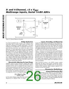
Figure 13. Ideal Unipolar Transfer Function, Single-Ended
Input, -FSR to 0
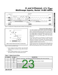
INPUT VOLTAGE (LSB [DECIMAL])
Figure 12. Ideal Bipolar Transfer Function, Single-Ended or
Differential Input
Selecting the Conversion Method
The conversion method is selected using the mode-
control byte (see the Mode Control section), and the con-
version is initiated using a conversion-start command
(Table 3, and Figures 2, 3, and 4).The MAX1032/
MAX1033 convert analog signals to digital data using one
of three methods:
FSR
3FFF
3FFE
3FFD
•
External Clock Mode, Mode 0 (Figure 2)
• Highest maximum throughput (see the Electrical
Characteristics table)
2001
2000
1FFF
• User controls the sample instant
• CS remains low during the conversion
• User supplies SCLK throughout the ADC con-
version and reads data at DOUT
0003
FSR x V
REF
16,384 x 4.096V
0002
0001
0000
1 LSB =
•
External Acquisition Mode, Mode 1 (Figure 3)
• Lowest maximum throughput (see the Electrical
Characteristics table)
0
1
2
3
8,192
INPUT VOLTAGE (LSB [DECIMAL])
16,381 16,383
• User controls the sample instant
(AGND1)
• User supplies two bytes of SCLK, then drives
CS high to relieve processor load while the
ADC converts
Figure 14. Ideal Unipolar Transfer Function, Single-Ended
Input, 0 to +FSR
• After SSTRB transitions high, the user supplies
two bytes of SCLK and reads data at DOUT
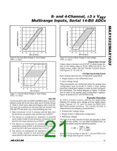
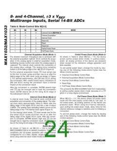
Mode Control
The MAX1032/MAX1033 contain one byte-wide mode-
control register. The timing diagram of Figure 15 shows
how to use the mode-control byte, and the mode-con-
trol byte format is shown in Table 7. The mode-control
byte is used to select the conversion method and to
control the power modes of the MAX1032/MAX1033.
•
Internal Clock Mode, Mode 2 (Figure 4)
• High maximum throughput (see the Electrical
Characteristics table)
• The internal clock controls the sampling instant
22 ______________________________________________________________________________________

 MAXIM [ MAXIM INTEGRATED PRODUCTS ]