8- and 4-Channel, 3 ꢀ ꢁREF
Multirange Inputs, Serial 14-Bit ADCs
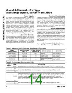
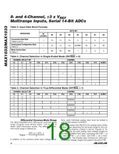
Table 3. Input Data Word Formats
DATA BIT
OPERATION
D7
(START)
D6
C2
C2
M2
D5
C1
C1
M1
D4
C0
C0
M0
D3
D2
0
D1
0
D0
0
Conversion-Start Byte
(Tables 4 and 5)
1
1
1
0
DIF/SGL
1
Analog-Input Configuration Byte
R2
0
R1
0
R0
0
(Table 2)
Mode-Control Byte
(Table 7)
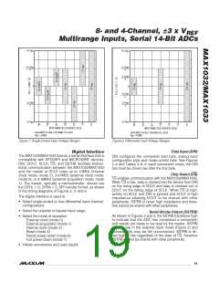
Table 4. Channel Selection in Single-Ended Mode (DIF/SGL = 0)
CHANNEL-SELECT BIT
CHANNEL
CH4
C2
0
C1
0
C0
0
CH0
CH1
CH2
CH3
CH5
CH6
CH7
AGND1
+
-
-
-
-
-
-
-
-
2/MAX103
0
0
1
+
0
1
0
+
0
1
1
+
1
0
0
+
1
0
1
+
1
1
0
+
1
1
1
+
Table 5. Channel Selection in True-Differential Mode (DIF/SGL = 1)
CHANNEL-SELECT BIT
CHANNEL
CH4
C2
0
C1
0
C0
0
CH0
CH1
CH2
CH3
CH5
CH6
CH7
AGND1
+
-
0
0
1
RESERVED
0
1
0
+
-
0
1
1
RESERVED
+
1
0
0
-
1
0
1
RESERVED
1
1
0
+
-
1
1
1
RESERVED
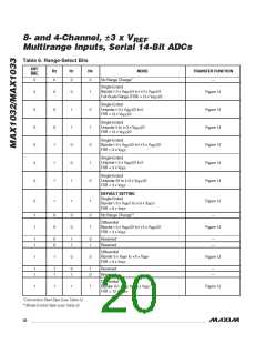
tions, each individual analog input must be limited to
16.5V with respect to AGND1.
Differential Common-Mode Range
The MAX1032/MAX1033 differential common-mode
range (V ) must remain within -14V to +9V to
obtain valid conversion results. The differential com-
mon-mode range is defined as:
CMDR
The range-select bits R[2:0] in the analog input config-
uration bytes determine the full-scale range for the cor-
responding channel (Tables 2 and 6). Figures 9, 10,
and 11 show the valid analog input voltage ranges for
CH_+ + CH_−
(
)
(
)
the MAX1032/MAX1033 when operating with FSR =
x V /2, FSR = 3 x V , and FSR = 6 x V ,
REF
3
V
=
CMDR
REF
REF
2
respectively. The shaded area contains the valid com-
mon-mode voltage ranges that support the entire FSR.
In addition to the common-mode input voltage limita-
18 ______________________________________________________________________________________

 MAXIM [ MAXIM INTEGRATED PRODUCTS ]