8- and 4-Channel, 3 ꢀ ꢁREF
Multirange Inputs, Serial 14-Bit ADCs
2/MAX103
t
CSPW
t
CSS
CS
t
t
t
CSH
CL
CH
SCLK
DIN
1
8
1
8
t
CP
t
DS
t
DH
START
SEL2
SEL1
SEL0
DIF/SGL
R2
R1
R0
START
M2
M1
M0
1
0
0
0
ANALOG INPUT CONFIGURATION BYTE
MODE CONTROL BYTE
t
t
TR
DV
HIGH
IMPEDANCE
HIGH
IMPEDANCE
HIGH
IMPEDANCE
DOUT
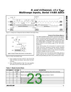
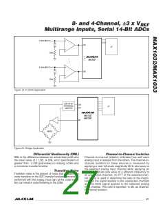
Figure 15. Analog Input Configuration Byte and Mode-Control Byte Timing
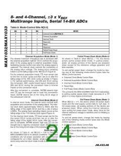
External Clock Mode (Mode 0)
The MAX1032/MAX1033’s fastest maximum throughput
rate is achieved operating in external clock mode.
SCLK controls both the acquisition and conversion of
the analog signal, facilitating precise control over when
the analog signal is captured. The analog input sam-
pling instant is at the falling edge of the 14th SCLK
(Figure 2).
SSTRB
t
SSCS
CS
SCLK
DOUT
t
CSS
Since SCLK drives the conversion in external clock
mode, the SCLK frequency should remain constant
while the conversion is clocked. The minimum SCLK
frequency prevents droop in the internal sampling
capacitor voltages during conversion.
t
DO
HIGH IMPEDANCE
MSB
SSTRB remains low in the external clock mode, and as a
result may be left unconnected if the MAX1032/
MAX1033 will always be used in the external clock mode.
NOTE: SSTRB AND CS REMAIN LOW IN EXTERNAL CLOCK MODE (MODE 0).
Figure 16. DOUT and SSTRB Timing
• User supplies one byte of SCLK, then drives CS
high to relieve processor load while the ADC
converts
• After SSTRB transitions high, the user supplies
two bytes of SCLK and reads data at DOUT
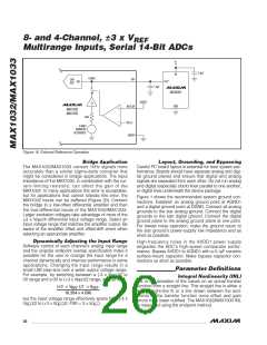
Table 7. Mode-Control Byte
BIT NUMBER
BIT NAME
DESCRIPTION
7
6
5
4
3
2
1
0
START
Start Bit. The first logic 1 after CS goes low defines the beginning of the mode-control byte.
M2
M1
M0
1
Mode-Control Bits. M[2:0] select the mode of operation as shown in Table 8.
Bit 3 must be a logic 1 for the mode-control byte.
Bit 2 must be a logic 0 for the mode-control byte.
Bit 1 must be a logic 0 for the mode-control byte.
Bit 0 must be a logic 0 for the mode-control byte.
0
0
0
______________________________________________________________________________________ 23

 MAXIM [ MAXIM INTEGRATED PRODUCTS ]