8- and 4-Channel, 3 ꢀ ꢁREF
Multirange Inputs, Serial 14-Bit ADCs
2/MAX103
This prevents the MAX1032/MAX1033 from inadvertent-
External Reference
For external reference operation, disable the internal
reference and reference buffer by connecting REFCAP
to AVDD1. With AVDD1 connected to REFCAP, REF
becomes a high-impedance input and accepts an
external reference voltage. The MAX1032/
MAX1033 can accept an external reference voltage of
4.096V or less. However, to meet all of the Electrical
ly exiting full power-down mode because of a CS glitch
in a noisy digital environment.
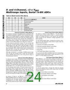
Power-On Reset
The MAX1032/MAX1033 power up in normal operation
configured for external clock mode with all circuitry
active (Tables 7 and 8). Each analog input channel
(CH0–CH7) is set for single-ended conversions with a
Characteristics specifications, V
must be > 3.8V.
REF
3 x V
bipolar input range (Table 6).
REF
The MAX1032/MAX1033 external reference current
varies depending on the applied reference voltage and
the operating mode (see the External Reference Input
Current vs. External Reference Input Voltage in the
Typical Operating Characteristics).
Allow the power supplies to stabilize after power-up. Do
not initiate any conversions until the power supplies
have stabilized. Additionally, allow 10ms for the internal
reference to stabilize when C
= 1.0µF and C
REFCAP
REF
= 0.1µF. Larger reference capacitors require longer
stabilization times.
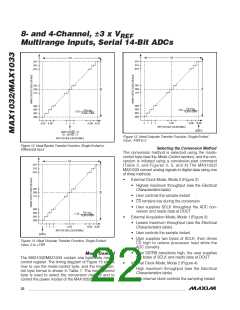
Applications Information
Noise Reduction
Additional samples can be taken and averaged (over-
sampling) to remove the effect of transition noise on
conversion results. The square root of the number of
samples determines the improvement in performance.
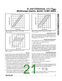
Internal or Eꢀternal Reference
The MAX1032/MAX1033 operate with either an internal or
external reference. The reference voltage impacts the
ADC’s FSR (Figures 12, 13, and 14). An external refer-
ence is recommended if more accuracy is required than
the internal reference provides, and/or multiple converters
require the same reference voltage.
For example, with 2/3LSB
(4LSB
) transition
P-P
RMS
noise, 16 (42 = 16) samples must be taken to reduce
the noise to 1LSB
.
P-P
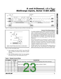
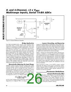
Internal Reference
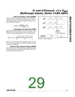
The MAX1032/MAX1033 contain an internal 4.096V
bandgap reference. This bandgap reference is connect-
ed to REFCAP through a nominal 5kΩ resistor (Figure 17).
The voltage at REFCAP is buffered creating 4.096V at
REF. When using the internal reference, bypass
REFCAP with a 0.1µF or greater capacitor to AGND1 and
bypass REF with a 1.0µF or greater capacitor to AGND1.
Interface with 0 to 10ꢁ Signals
In industrial-control applications, 0 to 10V signaling is
common. For 0 to 10V applications, configure the
selected MAX1032/MAX1033 input channel for the sin-
gle-ended 0 to 3 x V
input range (R[2:0] = 110,
REF
Table 6). The 0 to 3 x V
range accommodates 0 to
REF
10V where the signals saturate at approximately 3 x
V
if out of range.
REF
Interface with 4–20mA Signals
Figure 19 illustrates a simple interface between the
MAX1032/MAX1033 and a 4–20mA signal. 4–20mA sig-
naling can be used as a binary switch (4mA represents
a logic-low signal, 20mA represents a logic-high sig-
nal), or for precision communication where currents
between 4mA and 20mA represent intermediate analog
data. For binary switch applications, connect the
4–20mA signal to the MAX1032/MAX1033 with a resis-
tor to ground. For example, a 250Ω resistor converts
the 4–20mA signal to a 1V to 5V signal. Adjust the
resistor value so the parallel combination of the resistor
and the MAX1032/MAX1033 source impedance is
250Ω. In this application, select the single-ended 0 to 3
4.096V
REF
SAR
ADC
REF
1.0µF
0.1µF
1x
REFCAP
MAX1032
MAX1033
5kΩ
4.096V
V
RCTH
BANDGAP
REFERENCE
AGND1
x V /2 range (R[2:0] = 011, Table 6). For applications
REF
that require precision measurements of continuous
analog currents between 4mA and 20mA, use a buffer
to prevent the MAX1032/MAX1033 input from diverting
current from the 4–20mA signal.
Figure 17. Internal Reference Operation
______________________________________________________________________________________ 25

 MAXIM [ MAXIM INTEGRATED PRODUCTS ]