8- and 4-Channel, 3 ꢀ ꢁREF
Multirange Inputs, Serial 14-Bit ADCs
2/MAX103
12
12
8
8
4
4
0
0
-4
-8
-12
-16
-4
-8
-12
-16
-18
-12
-6
0
6
12
18
-18
-12
-6
0
6
12
18
INPUT VOLTAGE (V)
INPUT VOLTAGE (V)
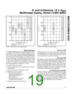
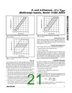
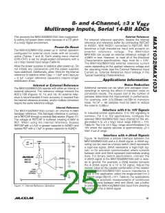
Figure 9. Common-Mode Voltage vs. Input Voltage
(FSR = 3 x V
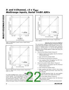
Figure 10. Common-Mode Voltage vs. Input Voltage
(FSR = 6 x V
)
)
REF
REF
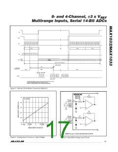
Output Data Format
12
8
Output data is clocked out of DOUT in offset binary for-
mat on the falling edge of SCLK, MSB first (B13). For
output binary codes, see the Transfer Function section
and Figures 12, 13, and 14.
4
0
Configuring Analog Inputs
Each analog input has two configurable parameters:
-4
-8
-12
-16
• Single-ended or true-differential input
• Input voltage range
These parameters are configured using the analog input
configuration byte as shown in Table 2. Each analog
input has a dedicated register to store its input configura-
tion information. The timing diagram of Figure 15 shows
how to write to the analog input configuration registers.
Figure 16 shows DOUT and SSTRB timing.
-18
-12
-6
0
6
12
18
INPUT VOLTAGE (V)
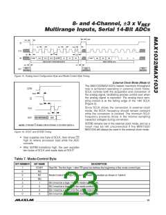
Figure 11. Common-Mode Voltage vs. Input Voltage
(FSR = 12 x V
)
REF
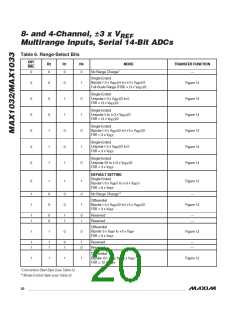
Transfer Function
An ADC’s transfer function defines the relationship
between the analog input voltage and the digital output
code. Figures 12, 13, and 14 show the MAX1032/
MAX1033 transfer functions. The transfer function is
determined by the following characteristics:
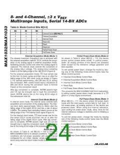
Start Bit
Communication with the MAX1032/MAX1033 is accom-
plished using the three input data word formats shown
in Table 3. Each input data word begins with a start bit.
The start bit is defined as the first high bit clocked into
DIN with CS low when any of the following are true:
• Analog input voltage range
• Single-ended or differential configuration
• Reference voltage
• Data conversion is not in process and all data from
the previous conversion has clocked out of DOUT.
• The device is configured for operation in external
clock mode (mode 0) and previous conversion-result
bits B13–B1 have clocked out of DOUT.
The axes of an ADC transfer function are typically in least
significant bits (LSBs). For the MAX1032/MAX1033, an
LSB is calculated using the following equation:
• The device is configured for operation in external
acquisition mode (mode 1) and previous conversion-
result bits B13–B5 have clocked out of DOUT.
FSR × V
REF
1 LSB =
N
2
× 4.096V
• The device is configured for operation in internal
clock mode, (mode 2) and previous conversion-
result bits B13–B2 have clocked out of DOUT.
where N is the number of bits (N = 14) and FSR is the
full-scale range (see Figures 7 and 8).
______________________________________________________________________________________ 21

 MAXIM [ MAXIM INTEGRATED PRODUCTS ]