8- and 4-Channel, 3 ꢀ ꢁREF
Multirange Inputs, Serial 14-Bit ADCs
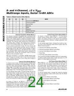
V+
1.0µF
IN
4.096V
REF
SAR
ADC
OUT
REF
1.0µF
MAX6341
GND
AVDD1
1x
REFCAP
MAX1032
MAX1033
5kΩ
4.096V
V
RCTH
BANDGAP
REFERENCE
AGND1
2/MAX103
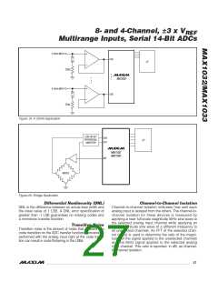
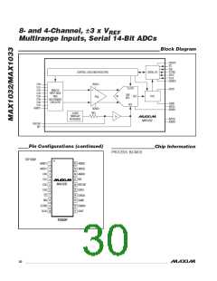
Figure 18. External Reference Operation
Bridge Application
The MAX1032/MAX1033 convert 1kHz signals more
accurately than a similar sigma-delta converter that
might be considered in bridge applications. The input
impedance of the MAX1032, in combination with the cur-
rent-limiting resistors, can affect the gain of the
MAX1032. In many applications this error is acceptable,
but for applications that cannot tolerate this error, the
MAX1032 inputs can be buffered (Figure 20). Connect
the bridge to a low-offset differential amplifier and then
the true-differential inputs of the MAX1032/MAX1033.
Larger excitation voltages take advantage of more of the
Layout, Grounding, and Bypassing
Careful PC board layout is essential for best system per-
formance. Boards should have separate analog and digi-
tal ground planes and ensure that digital and analog
signals are separated from each other. Do not run analog
and digital (especially clock) lines parallel to one another,
or digital lines underneath the device package.
Figure 1 shows the recommended system ground con-
nections. Establish an analog ground point at AGND1
and a digital ground point at DGND. Connect all analog
grounds to the star analog ground. Connect the digital
grounds to the star digital ground. Connect the digital
ground plane to the analog ground plane at one point.
For lowest noise operation, make the ground return to
the star ground’s power-supply low impedance and as
short as possible.
3 x ꢀ
/4 differential input voltage range. Select an
REF
input voltage range that matches the amplifier output. Be
aware of the amplifier offset and offset-drift errors when
selecting an appropriate amplifier.
Dynamically Adjusting the Input Range
Software control of each channel’s analog input range
and the unipolar endpoint overlap specification make it
possible for the user to change the input range for a
channel dynamically and improve performance in some
applications. Changing the input range results in a
small LSB step-size over a wider output voltage range.
High-frequency noise in the AꢀDD1 power supply
degrades the ADC’s high-speed comparator perfor-
mance. Bypass AꢀDD1 to AGND1 with a 0.1µF ceramic
surface-mount capacitor. Make bypass capacitor con-
nections as short as possible.
Parameter Definitions
For example, by switching between a (-3 x ꢀ
)/2 to
REF
Integral Nonlinearity (INL)
INL is the deviation of the values on an actual transfer
function from a straight line. This straight line is either a
best straight-line fit or a line drawn between the end-
points of the transfer function once offset and gain
errors have been nullified. The MAX1032/MAX1033 INL
is measured using the endpoint method.
0ꢀ range and a 0ꢀ to (+3 x ꢀ
)/2 range, an LSB is
REF
(+3 × ꢀ
) 2 × ꢀ
REF
REF
16,384 × 4.096
but the input voltage range effectively spans from (-3 x
)/2 to (+3 x ꢀ )/2, FSR = 3 x ꢀ ).
ꢀ
REF
REF
REF
26 ______________________________________________________________________________________

 MAXIM [ MAXIM INTEGRATED PRODUCTS ]