8- and 4-Channel, 3 ꢀ ꢁREF
Multirange Inputs, Serial 14-Bit ADCs
2/MAX103
+3 x V
+6 x V
REF
REF
+3 x V
2
+3 x V
REF
2
REF
+3 x V
2
REF
0
0
-3 x V
2
REF
-3 x V
2
-3 x V
2
REF
REF
-6 x V
-3 x V
REF
REF
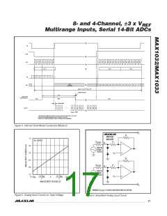
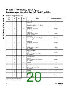
INPUT RANGE SELECTION BITS, R[2:0]
EACH INPUT IS FAULT TOLERANT TO 16.5V.
INPUT RANGE SELECTION BITS, R[2:0]
EACH INPUT IS FAULT TOLERANT TO 16.5V.
V
= 4.096V.
V
= 4.096V.
REF
REF
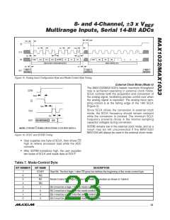
Figure 7. Single-Ended Input Voltage Ranges
Figure 8. Differential Input Voltage Ranges
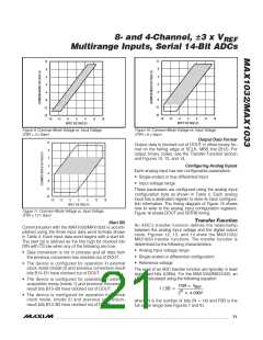
Data Input (DIN)
Digital Interface
The MAX1032/MAX1033 feature a serial interface that is
compatible with SPI/QSPI and MICROWIRE devices.
DIN, DOUT, SCLK, CS, and SSTRB facilitate bidirec-
tional communication between the MAX1032/MAX1033
and the master at SCLK rates up to 10MHz (internal
clock mode, mode 2), 3.67MHz (external clock mode,
mode 0), or 4.39MHz (external acquisition mode, mode
1). The master, typically a microcontroller, should use
the CPOL = 0, CPHA = 0, SPI transfer format, as shown
in the timing diagrams of Figures 2, 3, and 4.
DIN configures the conversion start byte, analog input
configuration byte and mode-control byte. See Figures
2–4 and Tables 3–8. In each conversion mode, the DIN
bits must be driven low after the first byte.
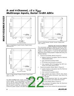
Chip Select (CS)
CS enables communication with the MAX1032/MAX1033.
When CS is low, data is clocked into the device from DIN
on the rising edge of SCLK and data is clocked out of
DOUT on the falling edge of SCLK. When CS is high,
activity on SCLK and DIN is ignored and DOUT is high
impedance allowing DOUT to be shared with other
peripherals. SSTRB is never high impedance and there-
fore cannot be shared with other peripherals.
The digital interface is used to:
• Select single-ended or true-differential input channel
configurations
• Select the unipolar or bipolar input range
Serial-Strobe Output (SSTRB)
As shown in Figures 3 and 4, the SSTRB transitions high
to indicate that the ADC has completed a conversion
and results are ready to be read by the master. SSTRB
remains low in the external clock mode (Figure 2) and
consequently may be left unconnected. SSTRB is dri-
ven high or low regardless of the state of CS, therefore
SSTRB cannot be shared with other peripherals.
• Select the mode of operation:
External clock (mode 0)
External acquisition (mode 1)
Internal clock (mode 2)
Reset (mode 4)
Partial power-down (mode 6)
Full power-down (mode 7)
• Initiate conversions and read results
______________________________________________________________________________________ 19

 MAXIM [ MAXIM INTEGRATED PRODUCTS ]