8- and 4-Channel, 3 ꢀ ꢁREF
Multirange Inputs, Serial 14-Bit ADCs
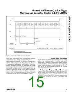
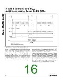
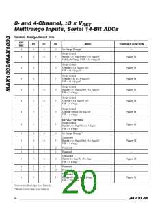
CS
SSTRB
SCLK
BYTE 1
BYTE 2
BYTE 3
BYTE 4
DIN
S
C2 C1 C0
0
0
0
0
***
HIGH
IMPEDANCE
DOUT
B13 B12 B11 B10 B9
B8
B7
B6
B5
B4
B3
B2
B1
B0
X
X
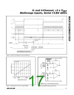
f
≈ f
SAMPLE SCLK
/ 32 + f
/ 17
INTCLK
1
SAMPLING INSTANT
t
ACQ
ANALOG INPUT
TRACK AND HOLD*
HOLD
TRACK
HOLD
100ns to 400ns
INTCLK**
f
≈ 4.5MHz
INTCLK
*TRACK AND HOLD TIMING IS CONTROLLED BY SCLK.
**INTCLK IS AN INTERNAL SIGNAL AND IS NOT ACCESSIBLE TO THE USER.
***DIN BYTES 2 TO 4 MUST BE DRIVEN TO LOGIC 0 TO OBTAIN A VALID CONVERSION.
Figure 3. External Acquisition-Mode Conversion (Mode 1)
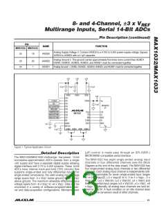
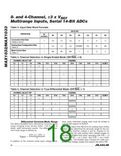
Figure 8 illustrates the software-selectable differential
analog input voltage range that produces a valid digital
output. Each analog input differential pair can be inde-
pendently programmed to one of three differential input
ranges by setting the R[2:0] control bits with DIF/SGL = 1.
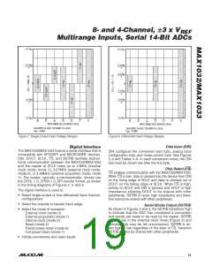
Any voltage beyond FSR, but within the 16.5V fault-
tolerant range, applied to an analog input results in a
full-scale output voltage for that channel.
Clamping diodes with breakdown thresholds in excess
of 16.5V protect the MAX1032/MAX1033 analog inputs
during ESD and other transient events (Figure 6). The
clamping diodes do not conduct during normal device
operation, nor do they limit the current during such
transients. When operating in an environment with the
potential for high-energy voltage and/or current tran-
sients, protect the MAX1032/MAX1033 externally.
Regardless of the specified input voltage range and
whether the channel is selected, each analog input is
16.5V fault tolerant. The analog input fault protection
is active whether the device is unpowered or powered.
16 ______________________________________________________________________________________

 MAXIM [ MAXIM INTEGRATED PRODUCTS ]