8- and 4-Channel, 3 ꢀ ꢁREF
Multirange Inputs, Serial 14-Bit ADCs
Power Supplies
To maintain a low-noise environment, the MAX1032/
MAX1033 provide separate power supplies for each
section of circuitry. Table 1 shows the four separate
power supplies. Achieve optimal performance using
separate AVDD1, AVDD2, DVDD, and DVDDO supplies.
Alternatively, connect AVDD1, AVDD2, and DVDD
together as close to the device as possible for a conve-
nient power connection. Connect AGND1, AGND2,
AGND3, DGND, and DGNDO together as close to the
device as possible. Bypass each supply to the corre-
sponding ground using a 0.1µF capacitor (Table 1). If
significant low-frequency noise is present, add a 10µF
capacitor in parallel with the 0.1µF bypass capacitor.
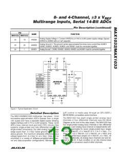
Track-and-Hold Circuitry
The MAX1032/MAX1033 feature a switched-capacitor
T/H architecture that allows the analog input signal to be
stored as charge on sampling capacitors. See Figures 2,
3, and 4 for T/H timing and the sampling instants for
each operating mode. The MAX1032/MAX1033 analog
input circuitry buffers the input signal from the sampling
capacitors, resulting in a constant analog input current
with varying input voltage (Figure 5).
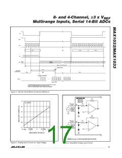
Analog Input Circuitry
Select differential or single-ended conversions using the
associated analog input configuration byte (Table 2).
The analog input signal source must be capable of dri-
ving the ADC’s 17kΩ input resistance (Figure 6).
Converter Operation
The MAX1032/MAX1033 ADCs feature a fully differen-
tial, successive-approximation register (SAR) conver-
sion technique and an on-chip T/H block to convert
voltage signals into a 14-bit digital result. Both single-
ended and differential configurations are supported
with programmable unipolar and bipolar signal ranges.
Figure 6 shows the simplified analog input circuit. The
analog inputs are 16.5V fault tolerant and are protect-
ed by back-to-back diodes. The summing junction volt-
age, V , is a function of the channel’s input common-
SJ
2/MAX103
mode voltage:
⎛
⎞
R1
R1 + R2
R1
R1 + R2
⎛
⎞
⎛
⎞
V
=
× 2.375V + 1+
× V
CM
⎜
⎝
⎟
⎠
⎜
⎝
⎟
⎠
SJ
⎜
⎟
⎝
⎠
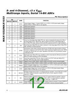
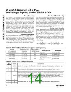
Table 1. MAX1032/MAX1033 Power Supplies and Bypassing
POWER
SUPPLY/GROUND
SUPPLY VOLTAGE
RANGE (V)
TYPICAL SUPPLY
CURRENT (mA)
CIRCUIT SECTION
BYPASSING
DVDDO/DGNDO
AVDD2/AGND2
AVDD1/AGND1
2.7 to 5.25
4.75 to 5.25
4.75 to 5.25
0.07
13.5
3.0
Digital I/O
0.1µF to DGNDO
0.1µF to AGND2
0.1µF to AGND1
Analog Circuitry
Analog Circuitry
Digital Control Logic and
Memory
DVDD/DGND
4.75 to 5.25
0.8
0.1µF to DGND
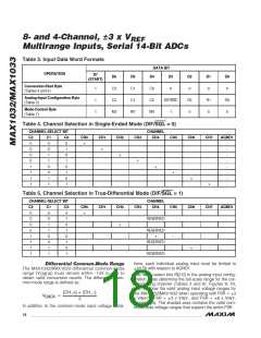
Table 2. Analog Input Configuration Byte
BIT
NAME
DESCRIPTION
NUMBER
7
6
5
4
START
C2
Start Bit. The first logic 1 after CS goes low defines the beginning of the analog input configuration byte.
Channel-Select Bits. SEL[2:0] select the analog input channel to be configured (Tables 4 and 5).
C1
C0
Differential or Single-Ended Configuration Bit. DIF/SGL = 0 configures the selected analog input channel
for single-ended operation. DIF/SGL = 1 configures the channel for differential operation. In single-ended
3
DIF/SGL mode, input voltages are measured between the selected input channel and AGND1, as shown in
Table 4. In differential mode, the input voltages are measured between two input channels, as shown in
Table 5. Be aware that changing DIF/SGL adjusts the FSR, as shown in Table 6.
2
1
0
R2
Input-Range-Select Bits. R[2:0] select the input voltage range, as shown in Table 6 and Figure 7.
R1
R0
14 ______________________________________________________________________________________

 MAXIM [ MAXIM INTEGRATED PRODUCTS ]